methods & tools
Our equipment at the EMRL in Aachen and Jülich comprises a broad spectrum of facilities for the fabrication and characterization of electronic materials and devices. The emphasis is placed upon oxide deposition technologies ranging from laser MBE, atomic layer deposition by MOCVD, high pressure sputtering to chemical solution deposition (CSD). These facilities are complemented by integration technologies such as optical and nanoimprint lithography, various metallization techniques, plasma based and ion beam based dry etching, as well as scanning probe based manipulation and self-assembly methods. In addition, we are equipped with a large variety of tools for the characterisation of processes, structures, and electronic properties. In particular, we provide a large range of dedicated scanning probe tools in order to analyze specific properties with atomic resolution. Circuit design is utilized for the development of hybrid and integrated circuits which comprise of new electronic functions as well as advanced measurement systems. Furthermore, our competences include numerical simulation and modelling methods which aim at the quantitative description of the electronic phenomena and materials under study as well as the corresponding devices.
The EMRL is a founding member of the section Fundamentals of Future Information Technologies of the Jülich-Aachen Research Alliance (JARA-FIT) and, as such, in addition to our own equipment, we have access through our partner institutes in the alliance to almost every conceivable nano-fabrication and nano-characterisation technique.
-
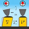
 JART – Juelich Aachen Resistive Switching Tools
Our laboratories provide simulation models for resistive switching devices to the scientific community. A focus on this dissemination activity are compact models to be used by circuit designers or device engineers. In the future, however, also kinetic Monte Carlo or continuum models will be provided. -
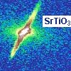
 The Electronic Oxide Cluster
Complex transition metal oxides and its heteroepitaxial interfaces have a large variety of exciting physical properties which could by employed in novel nanoelectronic devices. Due to its strong impact on the physical properties of complex oxides, one has to gain precise control ... (more) -
 Atomic scale deposition and self-assembly - electronic oxides and molecular systems
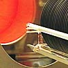
The EMRL provides a very wide spectrum of electronic oxide thin film deposition techniques. Our laser-based molecular beam epitaxy (laser-MBE) allows for the growth of heteroepitaxial oxide layers ... (more) -
 Probing the nanoworld - scanning probe techniques and more
Progress in nanoscience and nanotechnology is closely related to the evolution of novel techniques in experimental analysis. Tip-based scanning probe systems represent the work horses of our equipment at the EMRL for probing nanoscale structures ... (more) -
 Measurement techniques
Our laboratories provide a wide variety of general and dedicated measuring systems for the electrical characterization of electronic thin film materials and demonstrator devices under controlled conditions (temperature, atmosphere, bias voltage, ageing history, etc.) ... (more) -
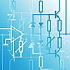 Circuit and system design
Analysis and design of circuits depends crucially on the utilisation of suitable tools for simulation and synthesis. The EMRL provides a professional infrastructure for the design and prototyping of measurement equipment at its disposal. This comprises design tools for ... (more) -
 Simulation and Modelling
Modelling on different scales and with a variety of approaches are performed for phenomena, materials, and devices. Model-based numerical simulations are employed using both, self-developed program modules and commercial standard tools. The approaches comprise ... (more) -
 Technological and analytical infrastructure