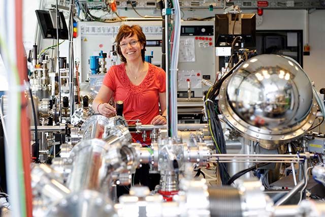
The Electronic Oxide Cluster
Complex transition metal oxides and its heteroepitaxial interfaces have a large variety of exciting physical properties which could by employed in novel nanoelectronic devices. Due to its strong impact on the physical properties of complex oxides, one has to gain precise control over lattice defects as well as over the valence state of the partially multivalent components. In order to tackle this challenging goal, we built up a UHV cluster-tool at the PGI-7 where we are combining a variety of complementary surface analysis tools in-situ with oxide-specific deposition methods e.g. pulsed laser deposition and sputtering in order to prevent surface oxidation and contamination. In particular, the analysis part of the cluster comprises scanning probes techniques (AFM, STM, LC-AFM, PFM), photoelectron spectroscopy (XPS) as well as photoelectron microspectroscopy (NanoESCA). Besides the growth of atomically tailored complex oxide thin films, the cluster tool provides the possibility to gain a deeper understanding of the nanoscale redox-processes which occur in oxides under electrical stimulus.
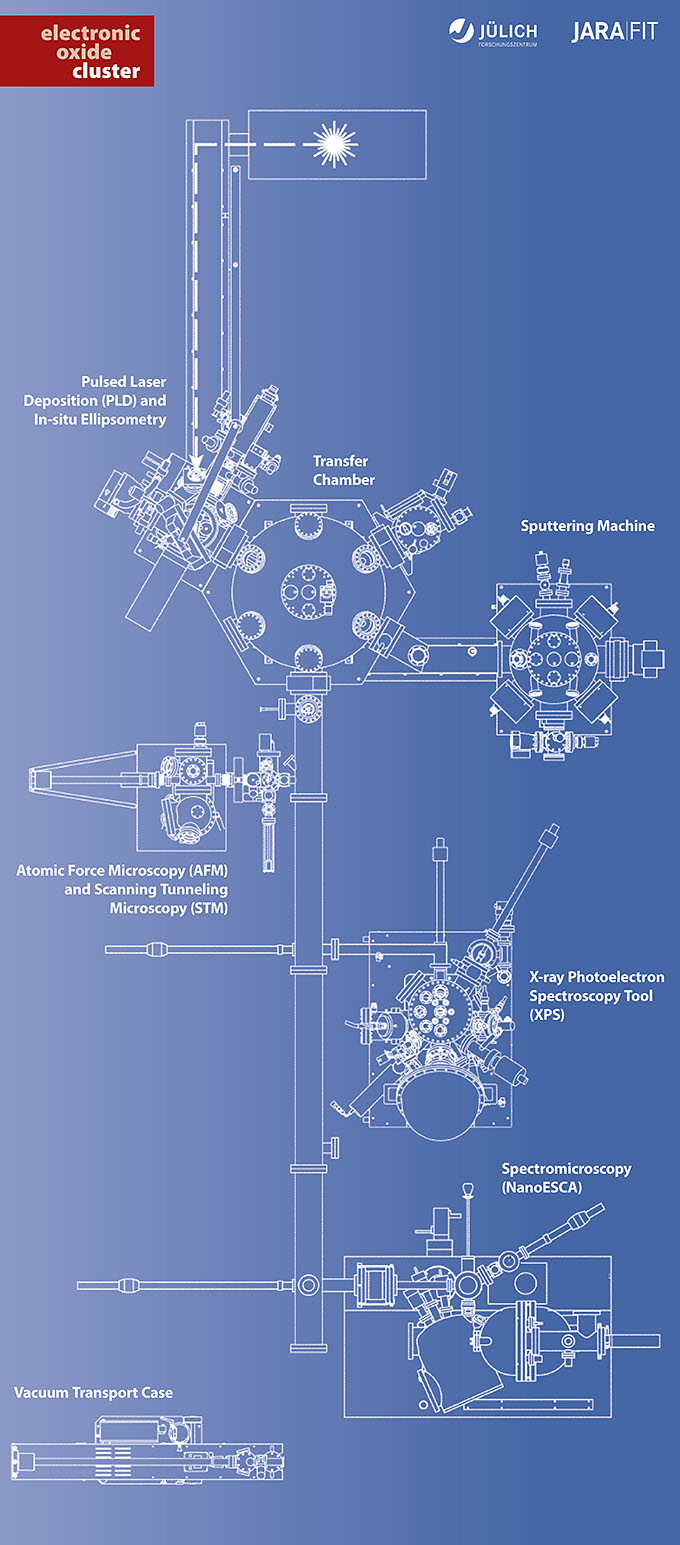
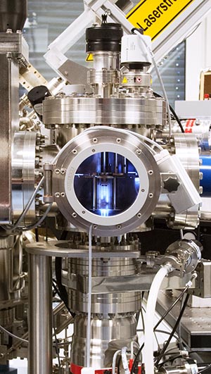
Pulsed Laser Deposition (PLD)
- Growth of epitaxial complex oxide thin films and heterostructures
- Atomically controlled growth by reflection high energy electron diffraction (RHEED) monitoring
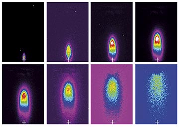
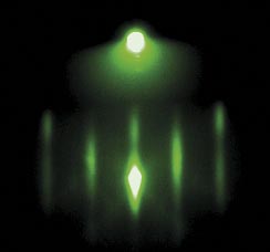
Time evolution of laser plume In cooperation with Dr. Amoruso from University of Naples
In-situ Ellipsometry of PLD Growth
Oblique incident reflectivity difference (OI-RD) system.
- Monitoring of optical and structural properties of thin films and heterostructures
- Formation and annealing of defects during growth
In cooperation with Prof. Zhu, University of California Davis
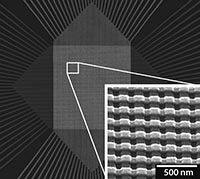
RHEED Pattern
Transfer Chamber
UHV transport between the different deposition chambers
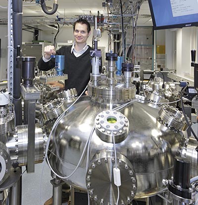
Sputtering Machine
- Deposition of metal electrodes
- Deposition of binary oxides
- Fabrication of oxide thin film devices on Si
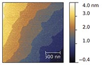
Variable Temperature Atomic Force Microscopy (AFM) and Scanning Tunneling Microscopy (STM)
- AFM non-contact mode
- Conductive tip AFM
- Piezo force microscopy
- Q+ sensor mode
- STM mode
- Ultrashort pulse mode

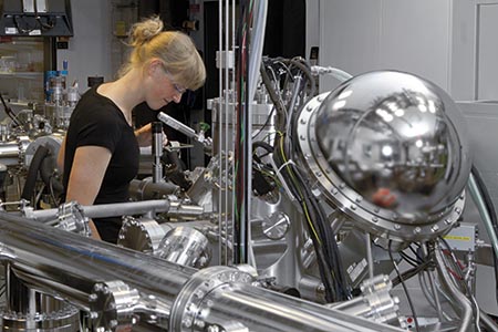
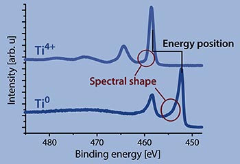
X-ray Photoelectron Spectroscopy Tool (XPS)
- High flux monochromatic X-ray source
- Valence band spectroscopy with UV-lamp
- Dual beam neutralization for insulating samples
- In-situ electrical manipulation
- Secondary electron imaging and chemical mapping
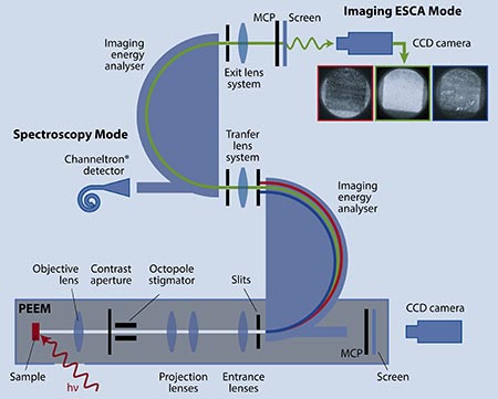
Spectromicroscopy (NanoESCA)
Spatially resolved chemical analysis of thin films and devices

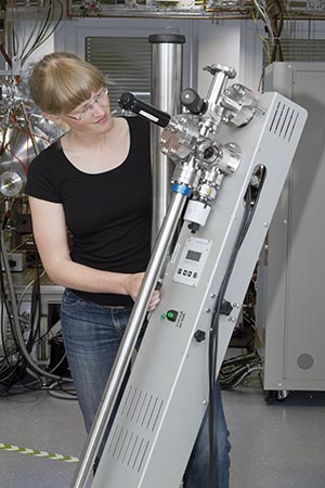
Vacuum Transport Case
UHV transport between the different deposition chambers