Atomic scale deposition and self-assembly - electronic oxides and molecular systems

The EMRL provides a very wide spectrum of electronic oxide thin film deposition techniques. Our laser-based molecular beam epitaxy (laser-MBE) allows for the growth of heteroepitaxial oxide layers, termination controlled interfaces, oxide superlattices, and artificial electronic oxides. Metal-organic chemical vapour deposition (MOCVD) including the atomic layer deposition from the vapour phase (ALD) is used for conformal coverage of micro- and nanoelectronic structures on chips by complex oxides. Multi-head high-pressure sputtering systems offer a versatile and flexible opportunity for the deposition of epitaxial oxide thin films. The chemical solution deposition (CSD) is a very flexible method mainly for producing polycrystalline or textured oxide films in the range from 50 nm to 5 m. In addition, our lab offers deposition techniques for molecular systems based on solution processes and UHV evaporation methods.
Laser MBE and Pulsed Laser Deposition of Oxide Thin Films
Methods
The pulsed laser deposition (PLD) technique is a powerful method for the deposition of multi-component materials, since it generally enables one to transfer the stoichiometry from a given ceramic or single crystalline target to the deposited thin film. The working principle of the PLD technique is displayed in Figure 1. A short, nanosecond range, pulse of an excimer laser beam is transferred via a suitable optical system to the rotating target. The laser pulse with a high energy of typically 2–5 J/cm2 lead to an evaporation of the target surface and the immediate formation of a plasma, containing energetic neutral atoms, ions and molecules. This so-called “plume” reaches the substrate surface with an energy of 0.1 to > 10 eV, depending on the pressure of the background gas environment. As a result of the short, high energetic laser pulses, the evaporated material is not in the thermodynamic equilibrium and the relative amount of different compounds in the plume corresponds to the target composition even for strongly-differing melting points. Therefore, in contrast to most other deposition techniques, the desired thin film stoichiometry can by easily achieved by PLD.
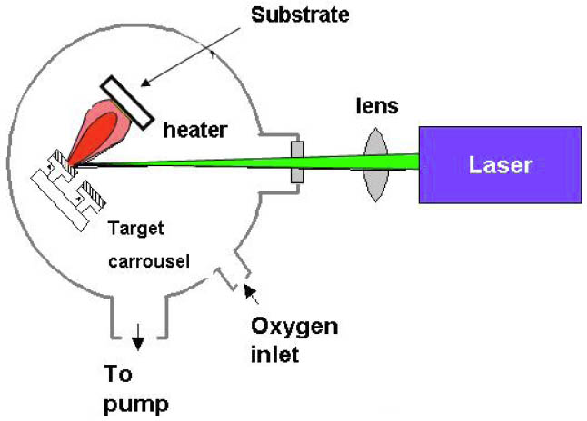
Figure 1: Schematic of Pulsed Laser Deposition
If reflection high energy electron diffraction (RHEED) is employed for in-situ monitoring during PLD, this method is often called Laser-MBE, since it provides a tool to control and adjust the growth on an atomic scale and to deposit sequences of single unit cells in a layer-by layer growth mode. The possibility to use building blocks of complex materials enables the design of artificial superstructures with atomically sharp interfaces with enhanced functionalities.
PLD laboratory
Our PLD lab (Figure 2) includes two conventional PLD systems (NEOCERA Inc.) and the Laser MBE UHV system (Twente Solid State Technology B.V.) equipped with a high-pressure RHEED tool. The beam of the Lambda physics excimer laser (LPX 300) is guided by a switchable mirror system to the 3 different chambers.
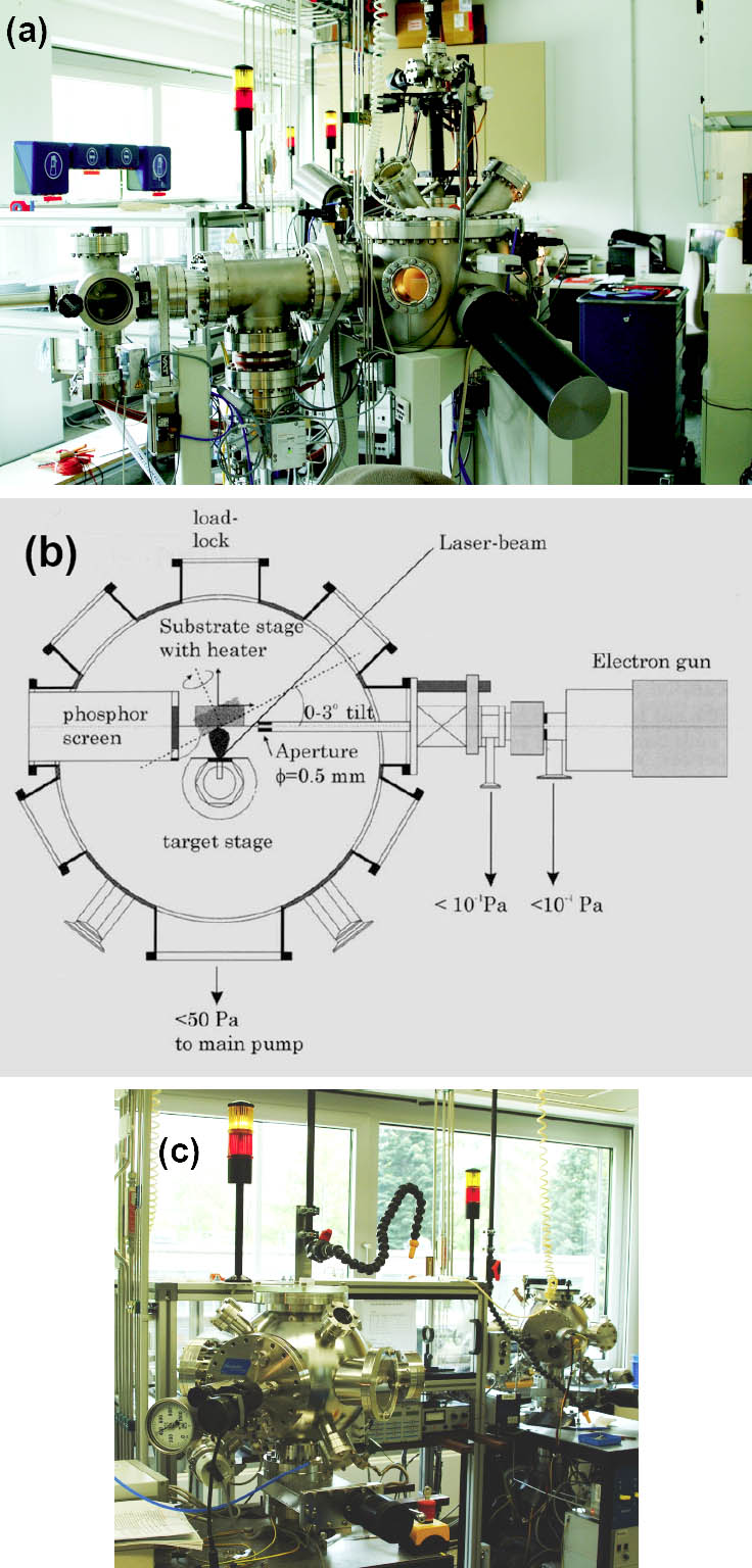
Figure 2: PLD lab: (a) Laser MBE system (b) drawing of the Laser MBE main chamber (c) The two conventional PLD chambers
Research
Pulsed Laser Deposition is employed for the fabrication of a large variety of complex oxide thin films with different functional properties, e.g. ferroelectrics, high-K-, as well as resistive switching materials.
The progress in understanding thin film growth by PLD, supported by sophisticated analysis techniques, e.g., RHEED, HRTEM and various scanning probe techniques enables us to control the growth of oxide hetero- and nanostructures on the atomic scale. Examples of our previous work are SrRuO3 nanowires, grown on LaAlO3 by self-assembling techniques, shown in Figure 3 and ultrathin heterostructures of SrRuO3 and BST fabricated by Laser MBE in an interval deposition mode. Figure 4 (c) shows the HAADF-STEM analysis of an 8-monolayer Ba0.7Sr0.3TiO3 (BST) thin film sandwiched between two SrRuO3 layers. The film thickness of the BST layer is homogeneous over larger areas and the interface is atomically sharp. The enlarged picture enables one to clearly identify the cations with the atomic columns. As an example for layered perovskite structures, we succeeded to grow the end member of the Ruddlesden-Popper phase SrO(SrTiO3)n by PLD from a stoichiometric target. Figure 5(c) shows a HRTEM picture of a Sr2TiO4 thin film with a perfect stacking order of SrO and STO layers.
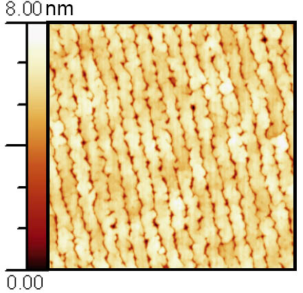
Figure 3: AFM measurement of self-assembled SrRuO3 nanowires on LaAlO3
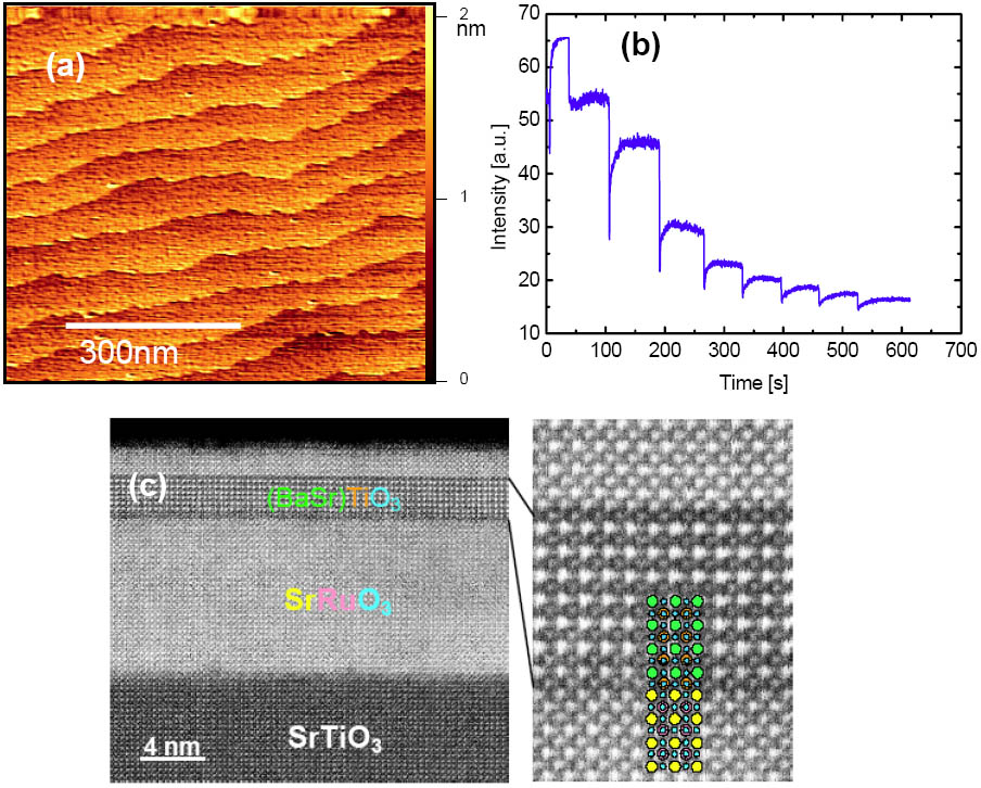
Figure 4: (a) AFM measurement of a 8 unit cell thick BaSr0.7Sr0.3TiO3 (BST) thin film; (b) RHEED oscillation during the growth; (c) HAADF-STEM analysis of a SRO/BST(8 monolayer)/SRO �heterostructure on STO. Within the enlargement on the right side, the atomic arrangement is sketched. �The colour code refers to the labels of the heterostructure on the left side.
Since the functional properties of oxide thin films are strongly influenced by the existence of defects, either point defects or extended defects, one key point of research is to gain a deeper understanding of the defect formation mechanisms during thin film growth. By choosing appropriate growth conditions, we succeeded to grow resistive switching thin films, containing regular arrays of resistive switching blocks, shown in Figure 5.
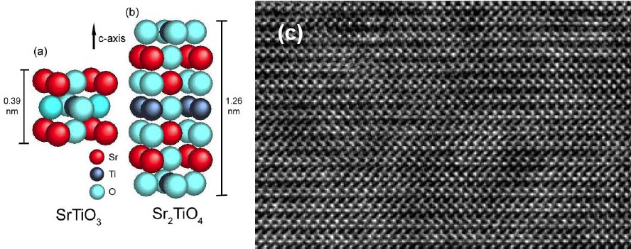
Figure 5: (a) Schematic of SrTiO3, (b) Schematic of Sr2TiO4, the end member of the Ruddlesden-Popper phase SrO(SrTiO3)n, (c) HRTEM picture of a highly ordered layered perovskite Sr2TiO4
R. Dittmann
Self-Assemby of Diblock-Copolymer Micelles for Template Based Preparation of PbTiO3 Nanograins
A bottom-up fabrication route for PbTiO3 nanograins grown on predefined TiO2 nanostructures used as seeds is presented. The structuring of the TiO2 seeds was performed using a self-organized template built up by a gold loaded micellar monofilm. With this fabrication process TiO2 seeds and PbTiO3 grains with a diameter of 12 nm and 30 nm, respectively, were prepared without any e-beam lithographic step. The dimensions of the structure imposed by the micelle template are transferred over all process steps to the final PbTiO3 grains. Furthermore it is shown that the inter-micelle distance and the degree of order in the dried monofilm is mainly determined by the preparation condition such as the pulling velocity in the dipping process and the strength of the surface-micelle interaction and not necessarily by the architectural properties (block length and ratio) of the diblock copolymers building the micelles. The inter-micelle spacing in the dried film is much smaller than the micelle dimension in solution and approaches the dimensions of a fully collapsed micelle in case the dipping process is performed slow enough.
The driving force in microelectronics industry is a continuous demand for cheaper and higher dense memories. In recent years especially ferroelectric or resistively switching perovskites have attracted considerable attention due to their potential for applications in non-volatile random access memories. But still there is a need for suitable fabrication processes of defined oxidic nanostructures with certain periodicity. Classical fabrication processes of defined nanostructures with certain periodicity are serial working, time consuming and thus expensive. Up to now some approaches exist which use hybrid top/down techniques based on templates or e-beam lithography to pattern nanograin structures which in a second step act as seeds for the deposition of ferroelectric or resistively switching perovskites by an additive technique [1, 2].
We realized a novel bottom-up fabrication route for PbTiO3-grains with natural grown facets based on predefined TiO2 nanostructures created by using a self-organized template. For details see Reference [3]. The process is schematically shown in Figure 1. The first steps of the preparation process involve the formation of micelles from A-B diblock copolymers, poly(vinylpiridine)-b-poly(styrene) (PVP-b-PS), and the loading of the micellar core with Au salt. The micellar monolayer film is created on platinized silicon substrates with a titanium top-layer by a dip coating process. The micelles arrange regularly in a hexagonal pattern. In the subsequent process step the organic compounds are removed by reactive ion beam etching (RIBE) with O2-plasma. The plasma treatment leads to a reduction of the Au salt and finally to one Au nanocluster per micelle by thermal annealing. The resulting Au nanoparticles are suitable as template for the structuring of the TiO2-thin film with reactive ion etching (RIE) using CF4-plasma. Subsequently the residual Au nanoparticles are removed by a RIBE Ar-plasma treatment step. In this way, TiO2 seeds are produced for the controlled growth of PbTiO3 nanograins by a chemical solution deposition technique. This additive growth technique results in crystals with natural growth facets.
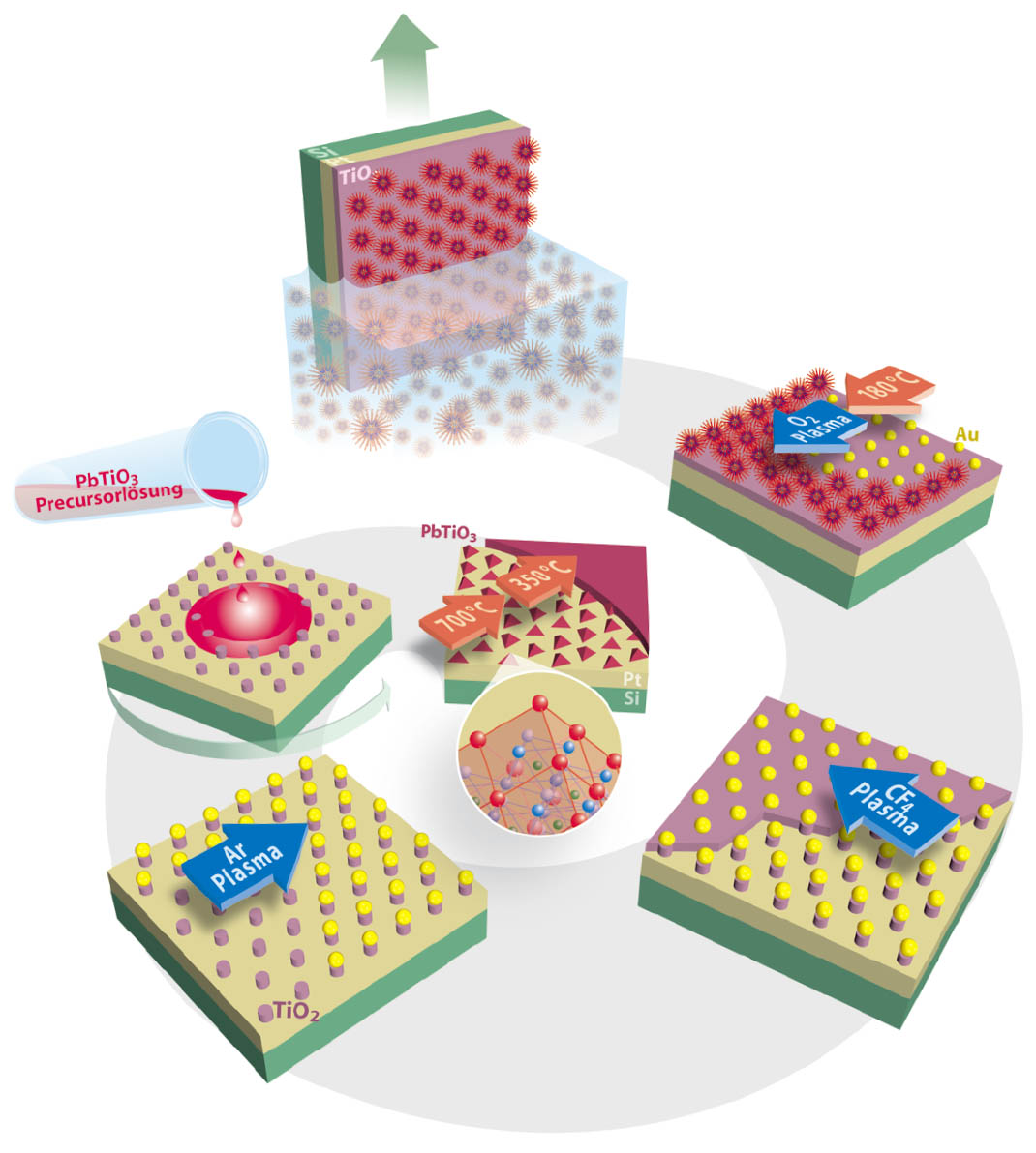
Figure 1: Process flow of the template based preparation of PbTiO3 nano-grains: (a) self- assembled gold loaded PVP-b-PS micelles, (b) gold nano-particles after reduction and temperature treatment, (c) gold covered TiO2 seeds after RIE, (d) elimination of the Au template by RIE and (e) PbTiO3 grains grown on TiO2 seeds.
The developed process route enables the fabrication of TiO2 seeds with a diameter of 12 nm, which can be used as nucleation sites for the growth of PbTiO3 nanograins having a diameter of only 30 nm and an average spacing of 55 nm. In contrast to other top-down assisted approaches [1, 2] leading to PbTiO3 nanograins with diameters > 50 nm, no time consuming and thus expensive e-beam lithography step is involved. Figure 2 shows the scanning electron photographs and inter-particle distances obtained from line scans taken for samples at different steps of the preparation process. Obviously, the structure dimensions can be transferred from the micellar template over all process steps to the final PbTiO3 nanograins.
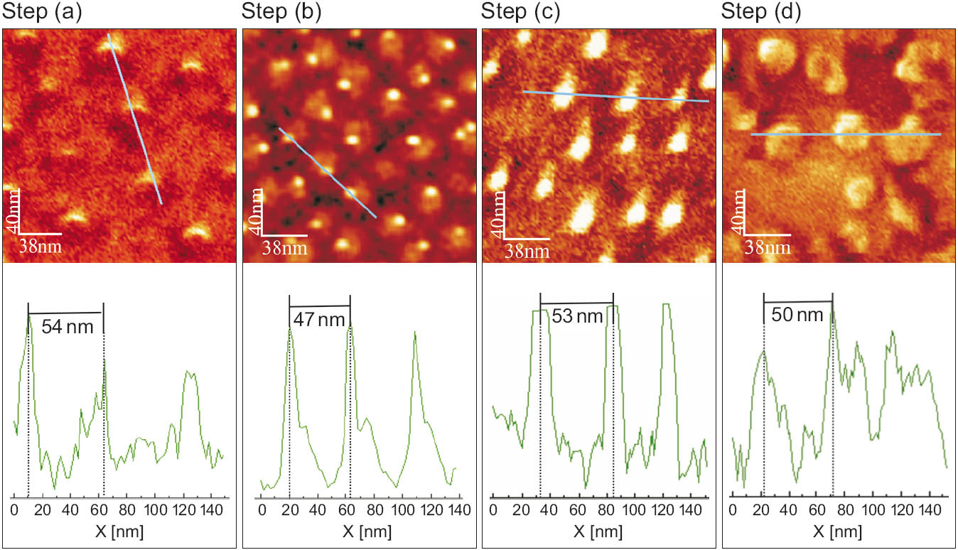
Figure 2: SEM photographs and results of line scans yielding the inter-particle distances taken at process steps (a), (b), (c) and (e) (see Figure 1) during the preparation of PbTiO3 nanograins on a TiO2 surface. For the monofilm preparation a pulling velocity of v = 5 mm/min was used.
The quality of the template is essential for the preparation process. The great interest of using diblock-copolymer micelles as templates was partly based on the idea that the spacing can be easily varied by increasing the length of the block building the shell. By a combined approach of scattering experiments on the solution properties of the Au loaded micelles and surface characterizations of the dried monolayer films we were able to work out which impact the diblock-copolymer architecture and the monolayer film preparation conditions have on the characteristics of the template. We did light scattering and also small-angle neutron scattering to obtain information about the full form factor which allows us to determine the overall shape of the micelles in solution and the distribution of the gold load in the micelles. In Figure 3 the density and mass distribution of a polymer micelle in solution and the gold distribution in the core for various gold loads are shown. The gold nucleus grows from the center and for the highest possible load the gold is evenly distributed all over the core. We compared the micelle dimensions and average inter-micelle spacing in solutions with those obtained from dried monolayer films. The inter-micelle spacing in the dried film is much smaller than the micelle dimension in solution and approaches the dimension of a fully collapsed micelle in case the dipping process is performed slowly enough. The micelles collapse, but they still have a certain mobility to rearrange on the surface during the drying process resulting in a higher degree of order of the pattern. It turned out that inter-micelle distances and the degree of order of the dried monofilm is mainly determined by the preparation condition such as the pulling velocity in the dipping process and the strength of the surface-micelle interaction and not necessarily by the architectural properties of the diblock copolymers building the micelles.
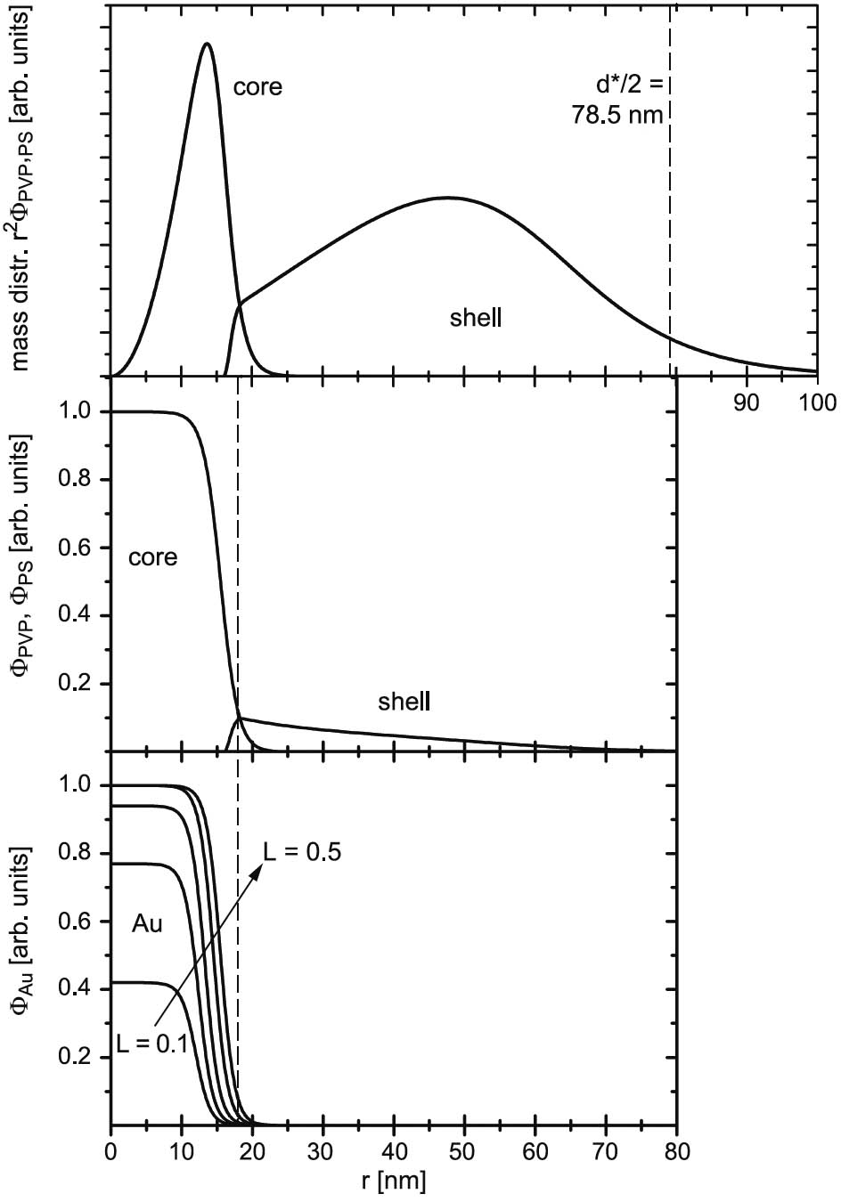
Figure 3: Density profile obtained by a simultaneous core-shell model fit of the form factors measured by small-angle neutron scattering for PS-b-PVP micelles with different gold loads. The upper part shows the density profiles for the PVP core and PS shell, respectively. In the lower part the gold distribution are shown. The insert shows the mass distribution of the unloaded micelles.
- [1] S. Bühlmann, P. Muralt, S. Von Allmen, Appl. Phys. Lett. 84, 2614 (2004)
- [2] S. Clemens, T. Schneller, A. van der Hart, F. Peter, R. Waser, Adv. Mater. 17, 1357 (2005)
- [3] S. Kronholz, S. Rathgeber, S. Karthäuser, H. Kohlstedt, S. Clemens, T. Schneller, Adv. Funct. Mater. 16, 2346 (2006)
S. Karthäuser, S. Rathgeber1, S. Kronholz, H. Kohlstedt, S. Clemens, T. Schneller, R. Waser
1Max-Planck Institut for polymer science, Mainz
Solution-based deposition of PTO nanograins
Task
The increasing interest in ferroelectric thin films for Ferroelectric-Random-Access-Memory applications leads to the question: how small can a ferroelectric capacitor be and still have a stable switchable remanent polarization? Until now there are only some calculations predicting a transition from the ferroelectric phase to a superparaelectric phase having no polarization if the size of the ferroelectric grain becomes small enough. At this size the ferroelectricity as a collective phenomena is quenched and the material is no longer applicable for non volatile memories. It is of great interest to find this limiting size to be able to evaluate the achievable storage density for future memory devices using ferroelectric materials.
Approach
Most experimental studies of so called size-effects in ferroelectrics use a top-down approach starting with a dense ferroelectric thin film and then use E-beam or FIB methods to structure small devices. With the top-down approach it is difficult to distinguish between the real intrinsic size effects and effects induced by the processing steps. Furthermore to achieve structures in the range of several nanometers a big experimental effort is required and up to now the ferroelectric limit could not be reached with these methods. For these reasons we propose a bottom-up approach growing single ferroelectric grains on a silicon substrate. As model material for perovskite structures lead titanate (PbTiO3) thin films are investigated. A chemical solution deposition (CSD) method for the preparation of lead titanate thin films is modified to achieve separated single PbTiO3 grains in the size ranging from 200 nm to less than 20 nm. This method opens up the way to study intrinsic size effects of several ferroelectric materials using an easy deposition method without the need of sophisticated and expensive structuring methods. The piezoresponse force microscope (PFM) is applied in order to monitor simultaneously ferroelectric and topological properties of individual grains.
Results
The PTO nanograins were deposited onto Si/SiO2/TiO2/Pt substrates. The separated PbTiO3 grains have no predominant crystallographic orientation as proven by X-ray diffraction experiments.
Figure 1 shows a scanning electron microscope (SEM) image of a sample with grain sizes in the range of 20 nm to 200 nm. When we look at the size and height distribution of the separated PbTiO3 grains it is noticed that the grains larger than 50 nm have an average height of 10 nm (Figure 2). Smaller grains have a decreasing height. The smallest measured grain had a diameter of about 12 nm and the height was 2.4 nm.
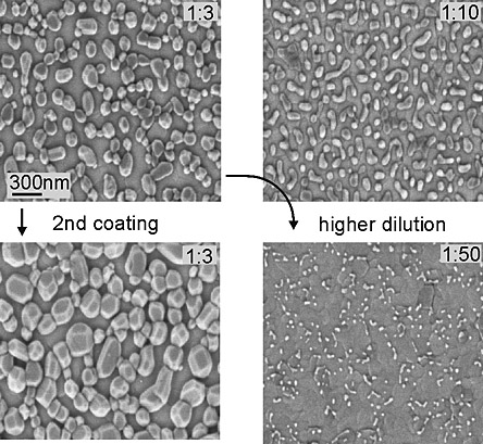
Figure 1: SEM micrographs of PTO single grains deposited by CSD using differently diluted precursor solutions (labeled in each micrograph). Additional coatings lead mainly to grain growth than an increase in the number of grains per area.
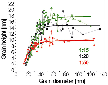
Figure 2: The grain height as a function of the grain diameter for three different precursor dilutions. The maximum grain height for larger grain diameters is correlated to the thickness of the amorphous film after the drying step.
Most fascinating is the finding represented in Figure 3. The topographic image clearly shows eight PbTiO3 grains of which two (marked with the white circles) do not lead to a piezoresponse signal as shown in the piezoresponse image Figure 3 (b) and (c). The grain volume can be estimated from the line-scans to be about 2400 nm3. We believe that (for this deposition method) at this grain-size the transition from the ferroelectric to the superparaelectric phase could take place. Accordingly a ferroelectric storage capacitor (based on these materials) smaller than 2400 nm3 would not function.
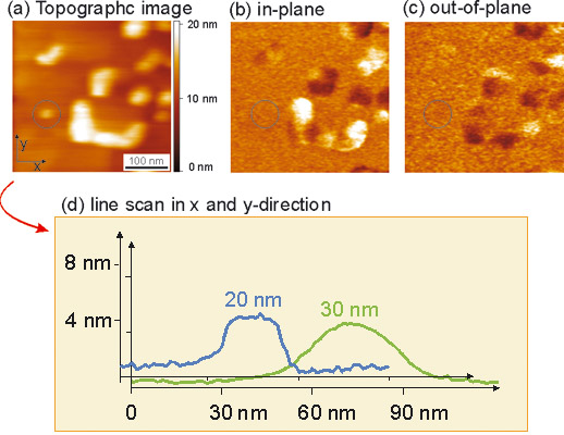
Figure 3: The topographical image (a) shows eleven PTO grains of sizes between 100 nm down to 20 nm indicated by the circle. In the PFM images (b) in-plane and (c) out-of-plane piezoresponse the smallest grain (marked with a circle) does not lead to any piezoresponse caused by the absence of the spontaneous polarization. (d) From the line-scans along x- and y-direction, the volume of the circled grains can be determined to be about 2400 nm3.
A. Roelofs
Nanoimprint Lithography for Crossbar Arrays
Nanoimprint lithography (NIL) is a powerful lithography method in the field of nanotechnology. Due to its high throughput, sub 10 nm resolution and low cost NIL is able to combine the advantages of conventional photo lithography and e-beam lithography in one tool [1]. In principle NIL works with a mold, which is pressed on a resist coated wafer to transfer the molds pattern into the resist layer. Now, we present first results of imprinted structures with a resolution of around 50 nm. Therefore thermal NIL as well as UV NIL is used. The molds are fabricated with e-beam lithography and reactive ion beam etching (RIBE).
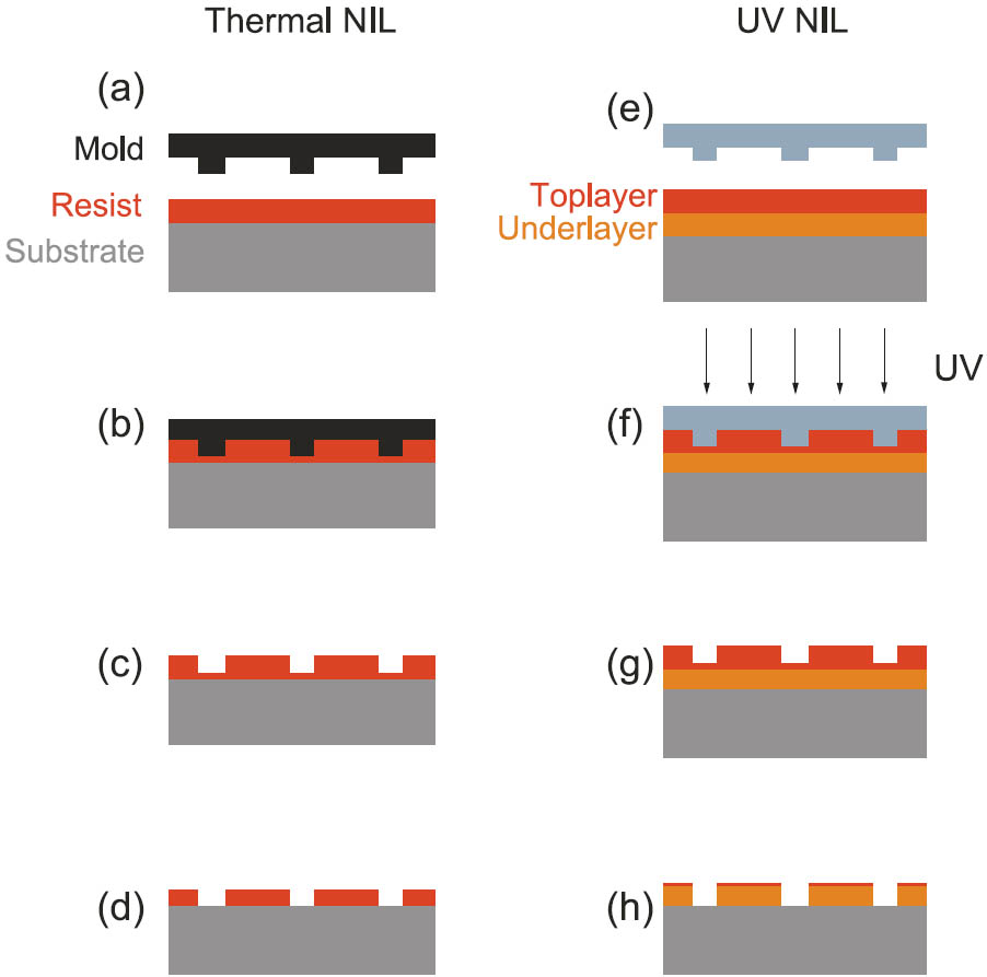
Figure 1: Process flow of thermal NIL and UV NIL
Concerning the limits of conventional lithography methods for the realisation of nanostructures, it is necessary to focus on an alternative tool. With nanoimprint lithography (NIL) it is possible to overcome the resolution limit of optical lithography in a high throughput process. Our aim is to realise nanocrossbar arrays for logic and memory devices with NIL [2]. Therefore it is aspired to imprint a couple of parallel wires scaled with a few nanometers as well as rectangular contact pads in the range of microns within one step only (Figure 2).
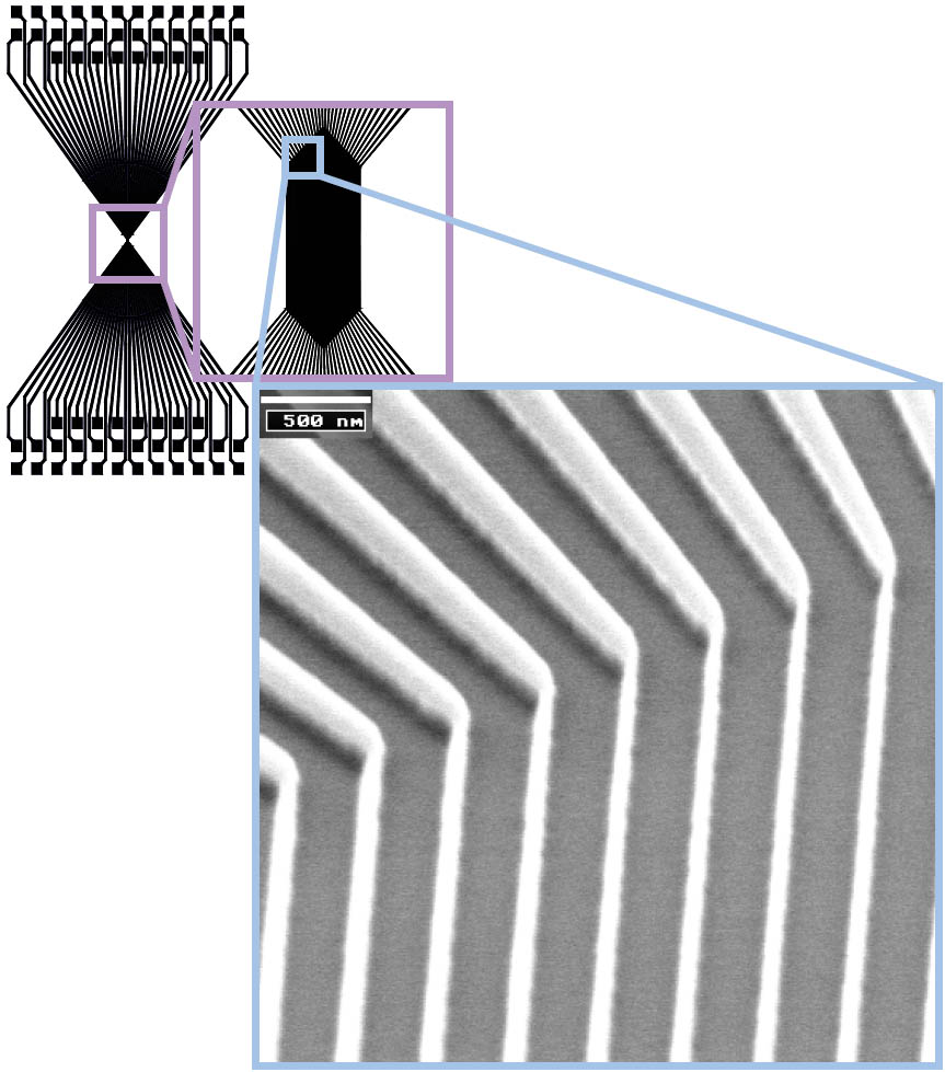
Figure 2: SEM image of a thermal NIL mold fabricated with e-beam direct writing and reactive ion beam etching (line width < 100 nm). The structure which was chosen for the image is schematically shown on the top. It pictures the bottom layer of a crossbar array structure (bottom electrode). Parallel lines in the dimension of nanometers define the centre of the array. Contact pads are needed for the electrical characterisation. The connection between the nanowires and the contact pads is realised by the so called fan out.
Dealing with NIL, it needs to be distinguished between thermal NIL and UV NIL. These two principles and their differences are shown in Figure 1. In both cases imprint resist is spinned on a substrate (Figure 1a and Figure 1e). In a thermal imprint process, the resist is heated above its glass transition temperature (Tg) and at the same time the mold is pressed into the resist layer (Figure 1b). Thus the resist gets deformed. Before removing the mold from the substrate the sample is cooled down below Tg, so that a replica of the mold stays in the hardened resist layer (Figure 1c). In a final step the residual layer on the bottom of the imprinted trenches needs to be removed, typically within a dry etching process (Figure 1d). For a UV imprint process a bi layer structure of resist is required. The top layer is photoactive whereas the under layer is more stable against etch processes and therefore suitable as etch mask. While pressing the transparent mold into the resist on the substrate the top layer resist is crosslinked by applying UV light (Figure 1f). After the release of the mold from the cured resist, the pattern is left in the top layer (Figure 1g), so that the under layer can get structured in a final dry etching process (Figure 1h). The most important advantage of UV NIL in comparison to thermal NIL is that there is no thermal impact during the process. Hence it is possible to handle temperature sensitive materials like organic molecules for example.
In the experiments a Nanonex 2000 imprint system is used for thermal NIL as well as UV NIL. The molds for thermal NIL are fabricated from silicon substrates with a silicon dioxide layer on the top which is structured by e-beam lithography and reactive ion beam etching (RIBE). Structures with a feature size of less than 100 nm and a height of around 110 nm are achieved (Figure 2). Some results of thermal imprint are shown in Figure 3. Very homogeneous nano lines and at the same time large rectangular structures (e.g. contact pads) are nicely transferred into the resist within one step. During the imprint process the temperature and the pressure are set to 150 ºC and 200 psi respectively.
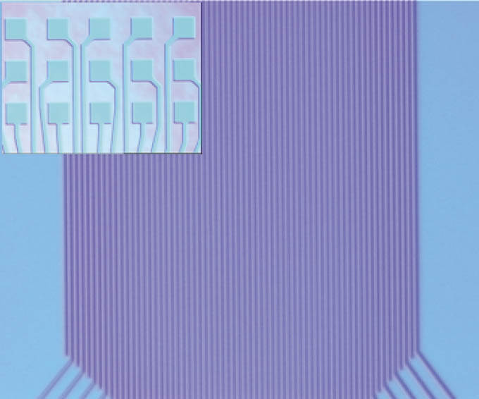
Figure 3: Optical microscope image of a structure, which was realised in a thermal NIL process (line width 500 nm). On the top are shown rectangular structures (100 μm × 100 μm contact pads), which are also printed very homogenously.
The molds for UV NIL are fabricated on transparent quartz glass substrates. Due to charging effects during e-beam direct writing it is necessary to evaporate a thin titanium layer on the quartz wafer. After e-beam lithography the metal layer is patterned by RIBE and acts as a hard mask in the following dry etch process to transfer the nanopattern into the substrate material. By this approach an UV imprint mold with structures in the range of 500 nm down to 50 nm and a depth of 100 nm to 200 nm can be realised.
It is beneficial to evaporate an anti adhesion layer (typically perfluorosilane) on the surface of the mold, to ensure a successful release of the mold from the substrate after the imprint process. Figure 4 shows a SEM image of UV imprinted lines with a resolution below 100 nm. The sidewalls of the structures are very steep, smooth and the aspect ration looks convincingly. Furthermore structures with a resolution down to 50 nm are achieved with UV NIL as it can be observed in Figure 5. At 20 ºC a pressure of 550 psi is typically applied to press the mold into the photo curable resist.
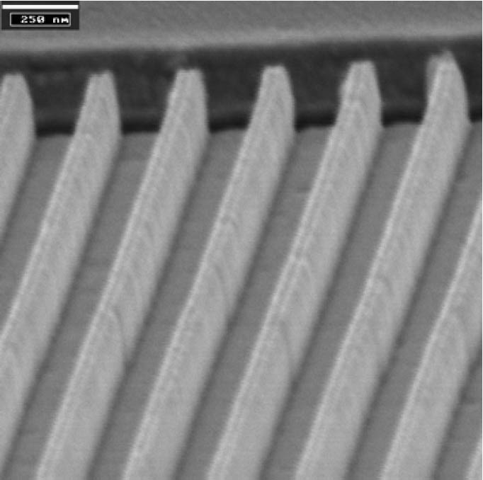
Figure 4: SEM image of UV imprinted structures. The resolution is below 100 nm with steep sidewalls and a high aspect ratio.
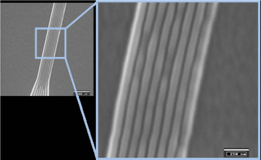
Figure 5: SEM image of UV imprinted structures. The line width is around 50 nm.
In conclusion we present the fabrication of molds for thermal and UV nanoimprint lithography by e-beam direct writing and reactive ion beam etching. Using those molds we realised structures down to 50 nm whereas at the same time large feature sizes in micrometer range are also imprinted.
- [1] S. Y. Chou, P. R. Krauss, P. J. Renstrom, J. Vac. Sci Technol. B 14, (1996)
- [2] G. Y. Jung, S. Ganapathiappan, D. A. A. Ohlberg, D. L. Olynick, Y. Chen, W. M. Tong, R. S. Williams, Nano Letters 4, 1225–1229, (2004)
M. Meier, C. Nauenheim, M. Prömpers, D. Mayer, C. Kügeler, R. Waser