Measurement techniques
Our laboratories provide a wide variety of general and dedicated measuring systems for the electrical characterization of electronic thin film materials and demonstrator devices under controlled conditions (temperature, atmosphere, bias voltage, ageing history, etc.). Our equipment includes, for example, ultra-broad band impedance analyzers, ferroelectric and piezoelectric hysteresis set-ups, a double beam laser interferometer with a resolution down to 0.1 pm (!), ultra-fast transient analyzers for a temperature range between 4 K and 1500 K, microwave network analyzers, semiconductor parameter analyzers, electrochemical potentiostats, etc. A range of dedicated measuring systems has been developed in our labs and led to the foundation of the company aixACCT Systems GmbH in the year 2000, which successfully develops, produces, and sells customer-specific advanced measurement equipment. Today, the emphasis of our own development activities at the EMRL lies on the design and realization of complex ultra-high resolution scanning probe systems for dedicated applications.
High Temperature Conductivity and Morphological Stability of SrTiO3 Thin Films
TASK
Leakage current and resistance degradation measurements of titanate based perovskites have shown significant differences between bulk and thin film behavior. In order to elucidate the dominant charge transport mechanisms, the defect chemistry and possible influences by surface effects, high temperature conductivity measurements on SrTiO3 thin films were performed as a function of temperature and oxygen partial pressure (pO2).
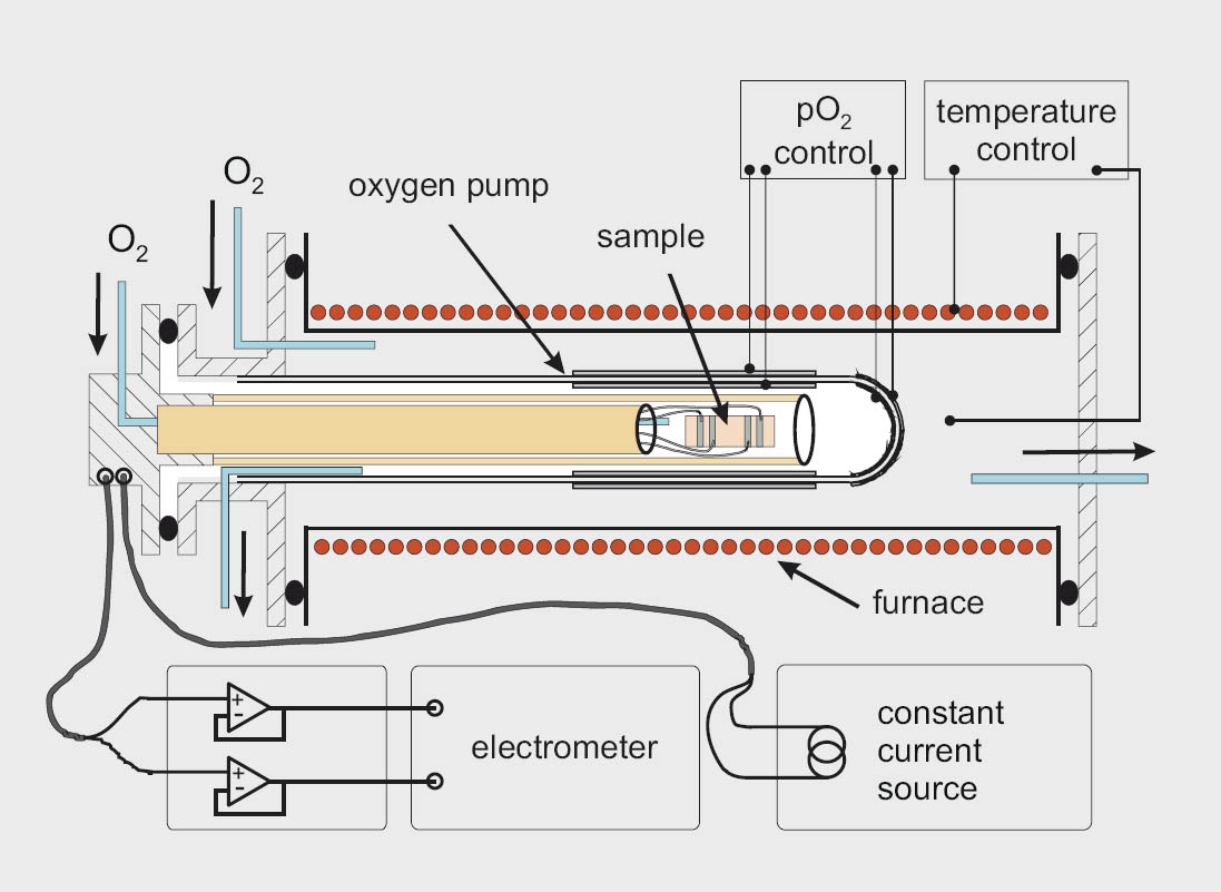
Figure 1: Schematic drawing of the high temperature conductivity measurement setup
APPROACH
Undoped and doped SrTiO3 thin films were grown on sapphire substrates using a CSD method. A 4-point-technique was employed to measure the resistances of the samples (typically up to several GΩ at 700 °C), thus avoiding the influence of the electrical contacts. To cope with the high resistance values the wiring was shielded triaxially. A solid state oxygen pump allowed to control the oxygen partial pressure in the range from approximately 10–20 bar to 1 bar for temperatures between 650 °C and 1000 °C.
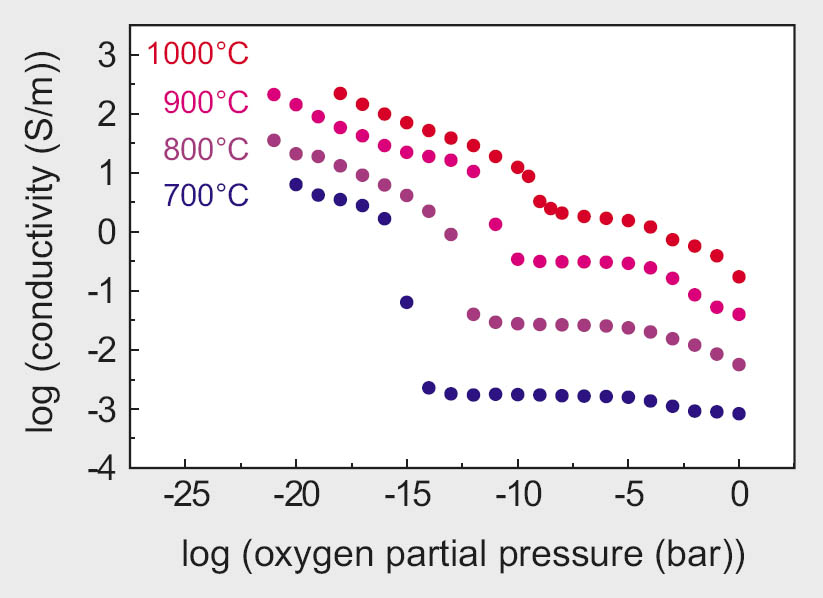
Figure 2: Conductivity of an undoped SrTiO3 thin film (d ∼ 500 nm) as a function of temperature and oxygen partial pressure
RESULTS
Investigations on a SrTiO3 single crystal and comparison with literature values demonstrated the capabilities of the experimental setup. First measurements on thin film samples indicate a significantly different conduction mechanism for SrTiO3 thin films compared to the conduction behavior of bulk ceramics.
Additionally, mass transport effects, activated under measurement conditions even at relatively low temperatures, lead to a restructuring of the morphology of the film indicating the formation of large extended defects. This renders the interpretation in terms of the well established bulk point defect chemistry very difficult and proves the investigation of conduction mechanisms of SrTiO3 thin films far more complex, especially due to the segrega-tion processes.
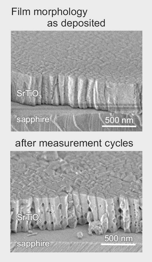
Figure 3: SEM micrographs of SrTiO3 thin film cross sections before and after measurement cycles showing an increasing porosity and surface roughness
Ch. Ohly, S. Hoffmann
Frequency Dependence of the Coercive Field in Ferroelectric Thin Film Capacitors for FeRAM Application
TASK
In ferroelectric single crystals, the time dependent polarization reversal is attributed to the nucleation and growth of domains of opposite polarity, as first intensively studied by Merz in the 50s. Ishibashi has used this approach to explain the frequency dependence of the coercive field, Ec, taking into consideration that the switching rate is determined by the applied field with an upper limit of the domain wall motion given by the velocity of sound. Due to the dimensions of ferroelectric thin films, the switching speed is too high to account for the frequency dependence of Ec observed in thin films (Larsen et al., 1994). Within this project, we aimed at an elucidation of the nature of this effect.
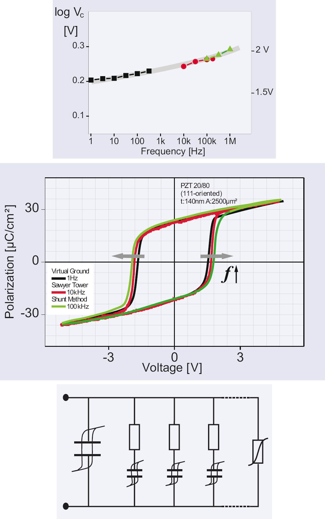
Figure 1: The frequency dependence of the coercive voltage of a PZT thin film capacitor and the describing equivalent circuit
APPROACH
Ec-f data found in the literature are typically limited to a frequency range of less than three orders of magnitude. In order to improve the data base, we employed a broad variety of techniques and succeeded to determine Ec in the range from approx. 10 mHz to more than 1 MHz. Furthermore, the current responses of voltage step stimulations are related to this frequency dependence.
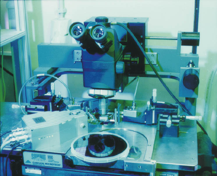
Figure 2: Probe station for characterizing structures on 6 inch wafers in the temperature range of −60 to +200°C
RESULTS
We found that the type of charge and discharge current responses are completely different from the curves found in single crystals. Rather, they can be interpreted by a Curie-von Schweidler type relaxation behavior. A re-consideration of the conventional switching theory of ferroelectric thin films leads to a consistent model based on the ferroelectric relaxation mechanism which is not related to the velocity of domain walls.
O. Lohse, M. Schumacher, D. Bolten, M. Grossmann, U. Böttger
Fast Pulse Switching Set-Up for Ferroelectrics
TASK
The coercive field and the remanent polarization are the characteristic values of the material for the design of an integrated FeRAM device. These vaules are required to be known at speeds equal to the speed ina real memory device because of the frequency dependence of the hysteresis loop.
The investigation of the switching behavior contributes to the knowledge (1) of theoretical values of the access time ofa FeRAM device that could be reached bya given material and (2) of loss mechanisms in the short time regime. In this project,a setup for investigating the switching behavior has been designed in order to emulate the FeRAM cell and to generate voltage pulses witha rise time in the 1ns-regime.
APPROACH
For emulating the FeRAM cell of the integrated circuit, the designated set-up needs to generate fast pulses of both polarities and to short the sample before starting the measurement. In order to meet these requirements,a concept based ona bridge circuit with a shunt resistor has been devised.
Both polarities can be generated depending on which switches of bridge circuit are activated.
An ultra-fast digital control unit has been built for precise timing withina pulse train and the correct repetition rate, usinga microcontroller in combination with high speed digital logic device families. The data lines were terminated to guarantee incident wave switching. Special care must be taken in selecting of the transistor, these devices are selected on the base of their low leakage current and small parasitic capacitance to optimize the switching velocity and signal quality.
A typical pulse train consists of a write pulse and two consecutive read pulses to investigate the switching and non-switching case of the polarization. The difference between these two current responses (switching and non-switching) has to be distinguished by the read amplifier of the integrated memory device.
RESULTS
The set-up showsa rise-time of the pulse-generator of 600 ps and an overall response time for recording the currents of less than 1 ns. If the current response of the pulse switching measurement is translated into a P(V)-curve,a significant difference of the coercive voltage between this curve and the hysteresis curve recorded by the standard low frequency excitation signal is found. The increase of the coercive voltage for the pulse switching test compared toa hysteresis loop recorded at 100 Hz amounts e.g. to factor of 1.6 for SBT thin films.
The difference in the current responses of the switching and non-switching case gives information on the access time of an integrated memory device.
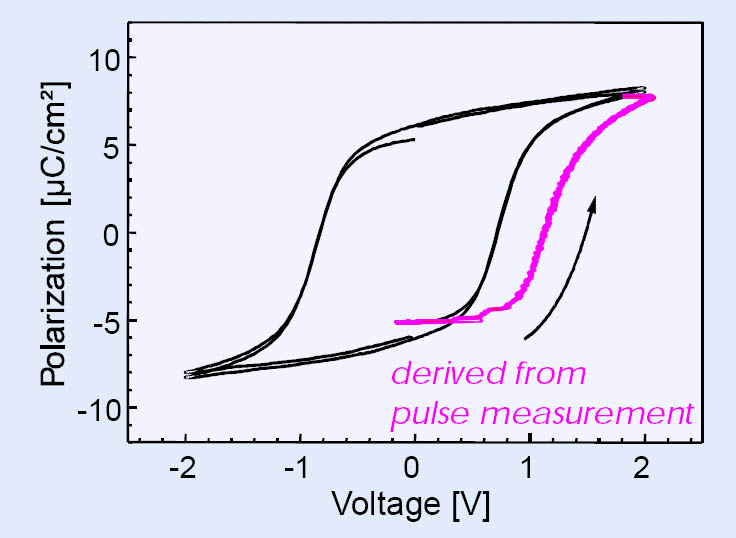
Figure 1: Increase in coercive voltage between low frequency excitation and pulse testing
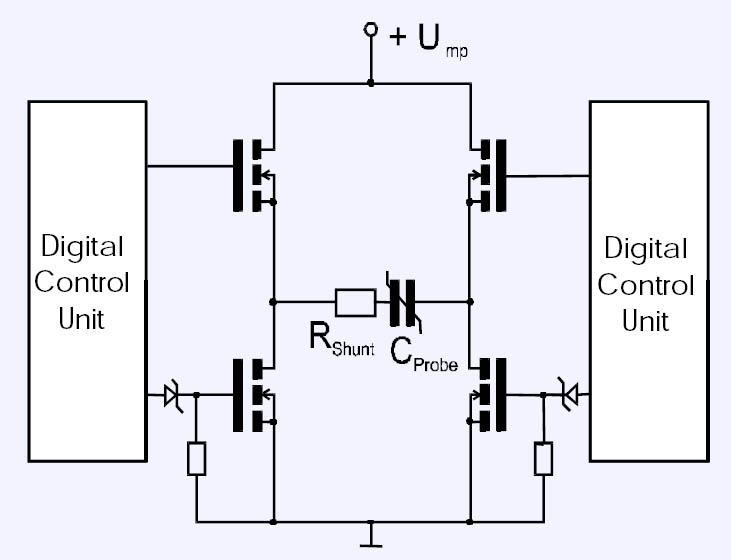
Figure 2: Equivalent Circuit of the Ulltra Fast Bridge Circuit
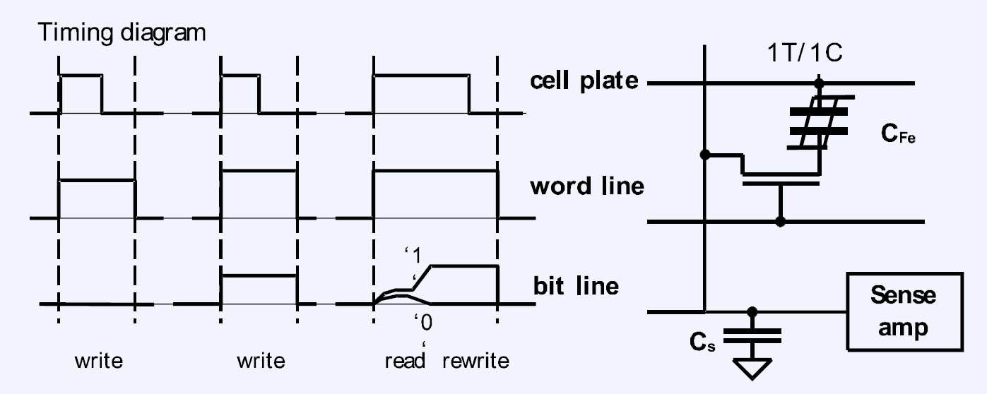
Figure 3: Typical timing diagram of a 1T/1C cell
O. Lohse, S. Tiedke, U. Kall
DRAM Emulation and Relaxation Current Measurement Set-Up
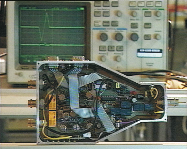
Figure 1: Prototype of the DRAM module
TASK
For the evaluation of high-k dielectric thin films for their feasibility in DRAM cells, dedicated measuring tech-niques are required. What is critical for the memory function is the voltage loss between refresh cycles for a capacitor which is first charged with a voltage pulse of a few 10 ns lengths and then opened. The voltage drop may be due to relaxation processes and to leakage currents. In order to identify the dominating process, the relaxation processes need to be determined over a wide dynamic range.
APPROACH
The DRAM pulse switch simulates the behavior of a storage cell in a memory device. This principle allows fast and easy detection of the suitability of a sample for DRAM application, because all relevant properties of a sample are measured with respect to the application.
A fast switch applies a short voltage pulse of adjustable length to the test capacitor simulating a write cycle with typically 5 ns rise time. To realize the complex digital circuitry required state-of-the art programmable logic devices (more than 10 k gates) were used. Multiple synchro-nously running Final State Machines (Mealy / Moore ) specified in VHDL ensure precise timing control to achieve high data acquisition rates.
The heart of the setup is the highly insulating, high-speed switch, which is essential for excluding the influence of the switch on the result. This part is realized as a double switch consisting of a highly insulating mechanical relay and a MOS transistor. The self-discharge process of the capacitor can be measured with negligible influence of the system due to the high impedance input resistance of the amplifier. Even so, the bandwidth of the electrometer rises to more than 10 kHz. The output voltage is then acquired and displayed by the aixACCT TF-Analyzer Basic Unit.
The relaxation current amplifier is used as a second characterization method. The relaxation current typically changes over several decades of magnitude in several decades of time, which makes it difficult to measure. One approach is to use a logarithmic current amplifier, which exploits a semiconduct-ors exponential characteristic to calculate an output proportional to the logarithm of the input current. This allows the current to be tracked over several decades. However, the principle is limited in speed, so for measurements in or below the microsecond range a variable linear amplifier has to be used, covering about three decades per stage. The charging or polarization current is measured while applying a fast voltage step with a previously selected level and amplifier stage, followed by a depolarization measurement by switching the voltage back to zero. This is also automatically controlled by the aixACCT TF-Analyzer Basic Unit.
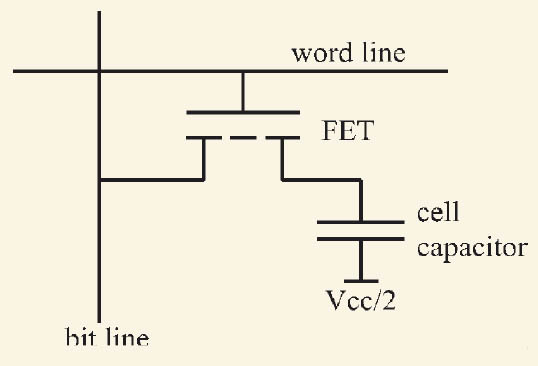
Figure 2: Schematic of a DRAM cell
RESULTS
During the APRA project, the DRAM pulse tests and the relaxation measurements were performed on a variety of BST thin films and related materials, both voltage and temperature dependent. The current response upon voltage step stimulation in the relaxation was found to be of the Curie-von Schweidler type in all cases, with varying slopes and magnitudes in the double log I-t plot. Using the Fourier transformation, the results have been related to the frequency independent loss tangent to evaluate the quality of the films.
In a real DRAM application, the relaxation leads to a fast decay of the initial capacitor voltage after a write pulse. However, it is difficult to predict the drop quantitatively because the (non-linear) leakage affects the voltage drop, too. A quick and easy way to 'see' these effects from the device point of view to use the DRAM pulse measurement. In direct comparison it can be seen, that the higher relaxation of a sample leads to a higher initial voltage drop, while the higher leakage current of the sample makes it drop lower at the end. A simulation model was established and applied to interrelate the DRAM emulation results, the relaxation processes, and the leakage currents in a quantitative manner. It is shown that the relaxation as well as leakage can have an important influence on the DRAM suitability of alternative high-k film materials.
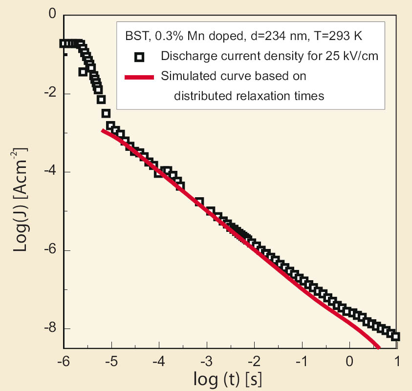
Figure 3: Measured and simulated discharge current densities of Mn-doped BST thin film
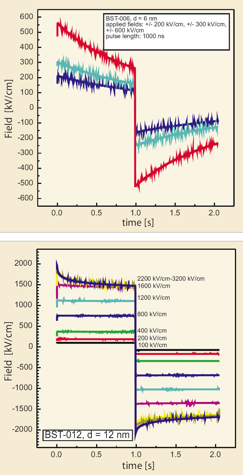
Figure 4: DRAM pulse measurements on samples BST-006 (thickness: 6 m) and BST-012 (thickness: 12 nm). Sample BST-012 showed excellent DRAM suitabilities up to 1.6 MV/cm.
T.Schmitz, S.Tiedke, M.Schumacher
Comparison of Microwave Measurement Techniques for Characterizing Dielectric Thin Films
TASK
The integration of novel dielectric materials like (Ba,Sr)TiO3 into high speed or high frequency applications (DRAM, controllable antennas, etc.) is of high interest. The investigation and characterization of these materials in the high frequency regime represents a challenging task and requires specialized measurement techniques. In literature, three ways for the determination of the dielectric constant and the loss factor of dielectric materials are often reported. Two of them characterize the properties of a sample capacitor via its reflection coefficient or a microstrip resonator technique, respectively. The third uses the complex propagation constant gathered from transmission line measurements. A comparison of these three techniques shows which are their main benefits and drawbacks.
APPROACH
Three different measurement techniques that are used to determine the well known high frequency properties of bare sapphire substrates are shown in Figure 1. In Figure 1a) the reflection coefficient of a sample capacitor is the basis for calculating its admittance over a broad frequency range. The measurement is performed with a network analyzer and on-wafer high frequency probe tips.
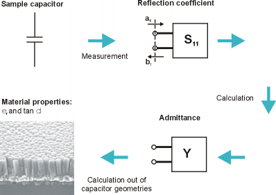
Figure 1a: Determination of material parameters via reflection coefficient measurement of a sample capacitor
The method presented in Figure 1b) is based on two equal microstrip resonators that are coupled with a flip-chip sample capacitor. The strong coupling causes the occurrence of a second resonant frequency near by the fundamental resonant frequency of the microstrip resonators. The ratio of these two
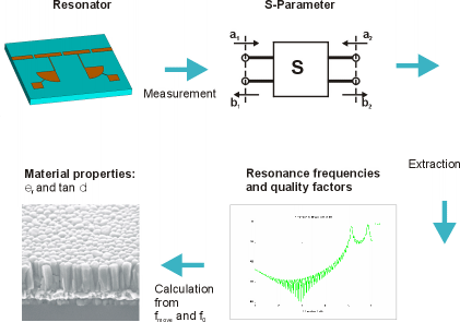
Figure 1b: Determination of material parameters via microstrip resonator technique
resonances determines the capacitance of the coupling capacitor. The loss factor is calculated from the influence of the capacitor on the resonance quality factor. The third technique (Figure 1c)) measures the phase difference of the S21 scattering parameter of two
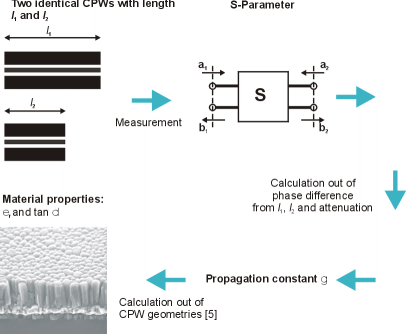
Figure 1c: Determination of material parameters from transmission line measurements
coplanar waveguides (CPW) with identical gap and signal trace sizes but different lengths. The phase difference of these two measurements correlates with the effective permittivity of the transmission line system and depends on the permittivity of the carrier-substrate and the geometric dimensions of the electrodes. The damping of the transmission line is correlated with the losses of the substrate and the resistivity of the electrodes. The layout of the sample structures for the described measurement setups is shown in Figure 2. Each structure has a planar electrode configuration to ensure good comparability between the three measurement techniques. Copper with a thickness of 3 µm is used for the electrode material.
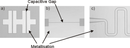
Figure 2: Sample layout: a) capacitor for reflection measurement b) flip chip capacitor c) CPW transmission line
RESULTS
A summary of the measurement results for the three setups is given Tab 1. The permittivity derived from the reflection coefficient measurement shows the worst accuracy with a deviation of 8.5 % from the literature value of 10.5. Against this the measurement error of the resonator and transmission line technique does not exceed a value of 2 %. In this context it must be mentioned, that the deembeding of
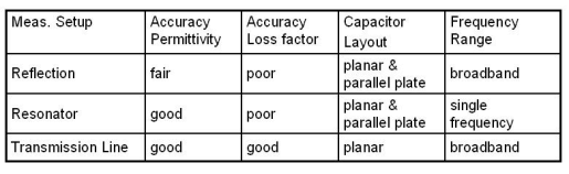
Table 1: Summary of the measurement accuracy
the network analyzer has a large impact onto the reflection measurement. Especially, a wrong positioned reference plane results in an additional phase offset that reflects in an error-prone capacitance value. The resonator and transmission line technique, however, are self-calibrating. Only the transmission line technique gives suitable results for the loss factor of the sapphire substrate. In the case of the reflection coefficient measurement the resolution of the network analyzer is not sufficient to determine the low loss factor of sapphire. The microstrip resonator technique suffers from the conductor losses of the microstrip resonators that mask the low losses of the coupling capacitor. Table 1 also summarizes the possible electrode configuration (planar, parallel plate) of the samples that can be investigated with the measurement setups and the frequency ranges that are covered.
S. Tappe, U. Böttger
High-Frequency Response of Ba0.7Sr0.3TiO3 Thin Films
Task
Thin Ba0.7Sr0.3TiO3 films (BST) are being intensivley studied for applications in voltage tunable high frequency devices like phase-shifters or tunable filters. In addition to the integration of these materials into existing device concepts their high frequency properties are still of major interest. Tunability, loss factor, temperature dependence and dispersion characteristics are important aspects from the device point of view.
Approach
Integrated BST thin film capacitors with electrode areas from (2 μm)2 to (40 μm)2 and film thicknesses between 100 nm and 250 nm are fabricated on highly resistive silicon substrates. A sketch of the BST thin film capacitor is shown in Figure 1.
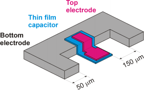
Figure 1: Schematic of the investigated BST thin film capacitors. The electrode configuration meets the requirements of high-frequency on-wafer testing
The physical layout meets the requirements for high-frequency on-wafer testing with air coplanar probe tips. The impedance spectrum of the capacitors is calculated from the reflection coefficient measured with a vector network analyzer. The effects of parasitic capacitance, inductance and resistance is eliminated with the help of open circuit and short circuit calibration structures on the silicon wafer. With this technique a frequency range up to 40 GHz is covered. To determined the tunability of the thin films a bias voltage ranging between −10 V and +10 V is applied.
Results
The capacitance spectrum of the investigated BST capacitors appears almost dispersion free up to 40 GHz without an applied bias field (Figure 2). With increasing the bias voltage a formation of resonances inside the capacitance spectrum is observed . Measurements on samples with different film thicknesses show that the position of the resonant frequencies is mainly controlled through the thickness of the BST films (Figure 4a).
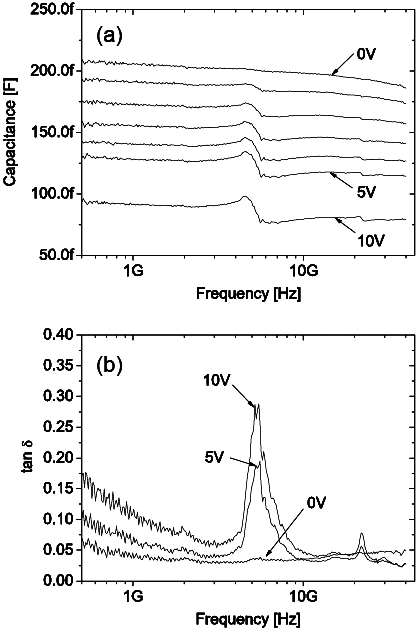
Figure 2: Capacitance spectrum (a) and loss spectrum (b) of a (4 μm)2 BST thin film capacitor at different bias voltages
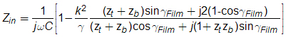
Although BST thin films are paraelectric at room temperature, their strong electrostrictive behavior enables the emission of bulk acoustic waves. Therefore it is assumed, that the BST thin film acts as a transducer element, that converts electrical energy into plane longitudinal acoustic waves traveling through the BST film, the top and bottom electrode and the substrate material. Thus, the resonance phenomena is determined through the acoustic properties and the dimension of each material layer incorporated in the BST capacitor. From transmission line theory the bounding acoustic impedances that are driven by the BST film are worked out. Then, the electrical input impedance of the capacitor can be calculated by means of the electro-mechanical coupling factor k of the BST film, the acoustic impedances zt and zb at the top and bottom of the BST film, and the propagation constant γFilm:
With this approach the capacitance spectrum of the investigated capacitors can be predicted, as shown in Figure 3. In addition the thickness dependence of the position of the resonant frequencies is calculated and a good agreement with the measurement is achieved (Figure 4).
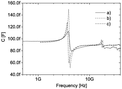
Figure 3: Measured a) and calculated (b), c))capacitance spectrum of a BST thin film capacitor. The calcualted graphs b) and c) are obtained for different values of the sound velocity of the BST thin film a) measurement, b) and c) calculation with different sound velocities of the BST thin film
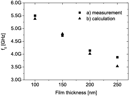
Figure 4: Measurement (a)) and calculation (b)) of the first resonant frequency depending on the BST film thickness
S. Tappe, U. Böttger