molecular electronics - concepts beyond the CMOS world
Specific organic molecules are capable of conduction and of storing single (or few) electrons which, in principle, can be controlled and manipulated. Molecules can be tailor-made by chemical synthesis in order to tune their electronic properties and to create nanometer-sized objects with dedicated electronic functionalities. In addition, they have the potential to self-organize on surfaces to regular 2-D patterns as well as to well-defined 3-D supramolecular objects. In fact, because of their tiny size to the order of one nanometer, they appear to be the ideal building blocks for designing future electronic devices with integration densities orders of magnitude beyond the CMOS concept of today. However, many fundamental questions have to be answered along the road of this evolution such as an unequivocal assignment of electronic functions to the molecular structure, controlled electronic contacts, molecular interconnects, etc. We are particularly interested in exploring the electron transport and storage properties of individual molecules. We investigate charge-controlled conformation changes, electronic interaction between metal nano-clusters and attached molecules, and excited states of cluster-molecule complexes for potential use as intramolecular logic gates. In cooperation with theory groups we achieve a complete quantum physical picture of the electronic behaviour of our molecular objects.
Chemical Tuning of π-Conjugated Molecules for Molecular Electronics
We have performed a combined experimental and theoretical study of several carboxylate molecules chemisorbed on the Cu(110) surface to investigate how to intentionally tune the electronic properties of such possible molecular electronic systems. By using the density functional theory (DFT) we predicted the electronic structure of single carboxylate-Cu(110) systems obtained by a systematic chemical functionalization process. For several carboxylate-surface systems, we carefully checked the predicted electronic structure by performing scanning tunnelling microscopy (STM) and scanning tunnelling spectroscopy (STS) experiments. On the basis of the experimental and theoretical data, molecular properties like the character (σ or π) of the individual molecular orbitals and the HOMO-LUMO gap variations caused by different substituents can be identified.
The development of future molecular electronic devices relies on a clear picture of the complex structure-physical property relationships present in molecule-surface systems [1]. To rationally design molecular electronic devices, a basic prerequisite is to understand how to specifically modify the electronic properties of a molecule-surface system in order to reach the desired device functionality. In this context, the theoretical tool of choice to predict the electronic structure of a molecule-surface system is DFT while experimentally it can be probed by STM and STS experiments.
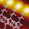
In a recent study [2] we have investigated how to change the electronic properties of a benzoate(C7H5O2) molecule chemisorbed on the Cu(110) surface by a systematic chemical functionalization process. As depicted in Figure 1, the electronic structure of the benzoate-Cu(110) surface can be rationally modified by (1) including an N atom in the aromatic ring, (2) by replacing an H atom at the aromatic ring by the carboxylic (COOH) functional group or by combining (1) and (2). As in depth discussed in [2], each functionalization path leads to fingerprint features of the calculated density of states (DOS) at the molecular site. For instance, one of the main differences between the possible functionalization paths, i.e. (1), (2) and (1+2), is how the hybridized molecule-surface states with a π character at the molecular site are located with respect to the Fermi level of the whole system (see reference 2 for more details). This knowledge can be further used either (i) to identify which specific carboxylate molecules are chemisorbed on a metal surface or (ii) to outline a practical scheme to design molecule-metal systems with specific transport properties.
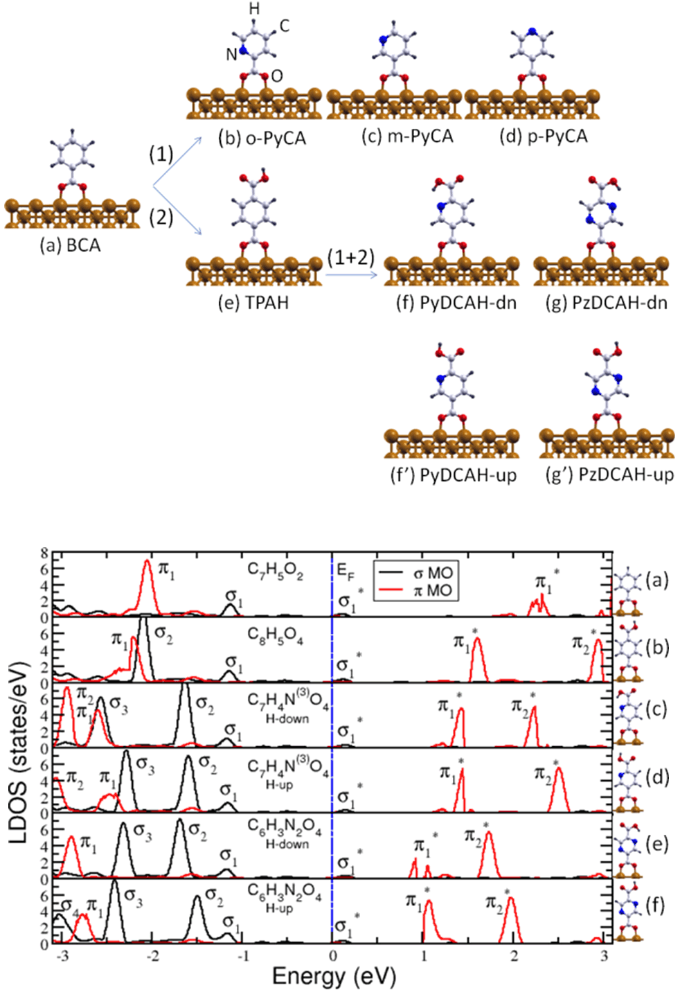
Figure 1:
(upper panel) Chemical functionalization process of (a) the benzoate (BCA) on the Cu(110) surface by (1) replacing a CH group in the aromatic ring through an N atom to obtain (b) ortho- (C6H4N(2)O2),(c) meta- (C6H4N(3)O2) and (d) para- (C6H4N(4)O2) pyridine carboxylate (PyCA) or by (2) replacing an H atom at the aromatic ring through a carboxylic group (COOH) resulting in (e) terephthalate (C8H5O4). Starting from (e) and further replacing a CH group by one N atom one obtains dehydrogenated pyridine-2,5-dicarboxylic acid (C7H4N(3)O4) with (f) or without an hydrogen bond (f'). A similar substitution in the latter system leads to dehydrogenated pyrazine-2,5-dicarboxylic acid (C6H4N2O4) also with (g) or without an hydrogen bond (g').
(lower panel) A characteristic feature of the density of states (DOS) calculated for the paths (2) and (1+2) is the shift of the unoccupied molecule-surface states with a π character at the molecular site closer to Fermi level.
The accuracy of the electronic structure predicted by the DFT calculations for the carboxylate-Cu(110) surface systems investigated in [2] can be experimentally verified via STS measurements. More specifically, the dI/dV spectra measured in STS experiments can be compared with the theoretical molecular density of states in order to identify for example the nature (σ or π) of the molecule-surface states at the molecular site. As an example, the molecule-surface states corresponding to the dI/dV peaks measured for the benzoate-Cu(110) surface system have a π character at the molecular site (see Figure 2). It is also interesting to note that the states with a σ character close to Fermi level like the bonding σ1 state does not appear as a clear feature in the dI/dV spectra. This fact is related to a lack of the charge density of this σ1 state at the molecule-vacuum interface.
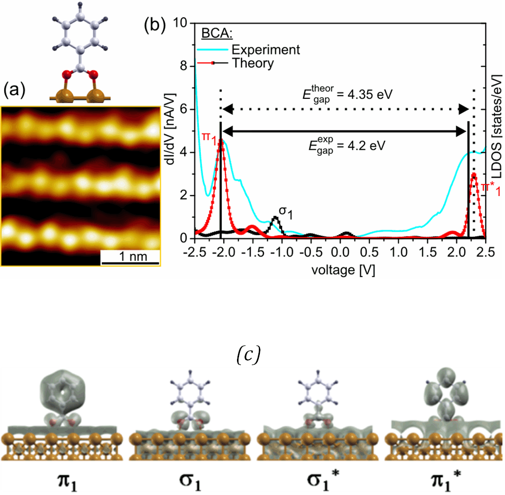
Figure 2: (a) High-resolution STM image of the BCA on Cu(110) surface. (b) The comparison between the experimental dI/dV spectrum recorded at a current set point of 0.5 nA and the theoretical DOS reveals that at the molecular site these peaks have a π character. Note that the molecule-surface states close to Fermi level with a σ character at the BCA site do not appear as a clear feature in the dI/dV curve. (c) Charge density plots of the molecule-surface states in an energy range corresponding to σ and π depicted in (b).
Furthermore, we have shown in a recent publication [3] that a careful analysis of the experimentally measured dI/dV curves in terms of the calculated DOS can reveal also the molecular structural changes that can occur during an STM/STS experiment performed for a molecule-surface system.
As shown in Figure 3, in the case of the pyridine-2,5-dicarboxylic acid on Cu(110) the height-dependent dI/dV curves measured for different values of the tunnelling current set points exhibit a peak structure characteristic for each STM-tip height. Interestingly, for this molecule on the Cu(110) substrate, several different conformers are possible controlled by the specific position of the H atom in the carboxylic group (COOH) at the vacuum interface. From theoretical point of view, for each of these possible conformers a fingerprint DOS can be calculated which unambiguously indentifies it. Then a careful comparison between the STS measurements and the theoretical DOS reveals that a different peak structure of the height-dependent dI/dV spectra can be assigned to different positions of the H atom in the carboxylic group. Besides this structural information our combined experimental and theoretical work also reveals, as already shown in the previous example, the character (σ or π) of the hybridized molecule-surface states at the molecular site as a function of the tip position.
Figure 3: Experimental dI/dV spectra vs calculated DOS for (dehydrogenated) pyridine-2,5-dicarboxylic acid on the Cu(110) surface. By increasing the tunneling current set point, some occupied molecule-surface states with a σ character at the molecular site like σ3 modify their energetic position relative to σ2 and π1 suggesting a molecular structural change. Depending on the STM tip height, the molecule-surface states spatially localized at different molecular parts can be also detected.
- [1] S. Karthäuser, J. Phys.: Condens. Matter. 23, 013001 (2010).
- [2] V. Caciuc, M. C. Lennartz, N. Atodiresei, S. Karthäuser and S. Blügel, Nanotechmoogy 22, 145701 (2011).
- [3] M. C. Lennartz, V. Caciuc, N. Atodiresei, S. Karthäuser and S. Blügel, Phys. Rev. Lett. 105, 066801 (2010).
V. Caciuc1, M. C. Lennartz, N. Atodiresei1, R. Waser, S. Blügel1, and S. Karthäuser
1 PGI-1: Peter Grünberg Institut - Quantum Theory of Materials
Arylthio-Substituted Coronenes as Tailored Building Blocks for Molecular Electronics
The electron transport through molecules in molecular devices is typically influenced by the nature of the interfaces with the contacting electrodes and by the interactions between neighbouring molecules. It is a major goal of molecular electronics to adjust the electronic function of a molecular device by tailoring the intrinsic molecular properties and the interfacial and intermolecular interactions. Here, we report on the tunability of the electronic properties of coronene derivatives, namely dodecakis(phenylthio)-coronenes (DPTCs), which are found to exhibit a three-dimensional aromatic system. Scanning tunnelling microscopy (STM), spectroscopy (STS) and simulations based on the density functional theory (DFT) are employed to characterize the structural and electronic properties of these molecules deposited on Au(111) surfaces. It is shown that modifications of the peripheral aryl-groups allow to specifically affect the self-assembly and the charge transport characteristics of the molecules. Molecular assemblies like supramolecular wires with highly delocalized orbitals and single molecules with molecular “quantum dot” characteristics are obtained in this way.
The development of future nanoelectronic devices based on single molecules or well-defined molecular assemblies is driven by the vision that a great variety of functionalities may be implemented by using the appropriate chemical design. In this study, we report on a molecular system based on a polycyclic aromatic hydrocarbon core, substituted thoroughly by phenylthio-groups, i. e. dodecakis-(phenylthio)coronene (DPTC). DPTC can be seen as nanosized system with a three-dimensional delocalized electronic network. Further systematic substitution of DPTCs, i. e. with electron-with-drawing trifluoromethyl-moieties or electron-donating methoxy-moieties, leads to the compounds DFPTC and DMPTC, respectively [1].
The monolayer of DFPTC deposited on Au(111) shows ordered domains consisting of parallel chains which are surrounded by a disordered region. The columnar arrangement of DFPTC (Fig. 1(a)), is in line with findings made for discotic liquid crystals. Molecules with strongly electronwith-drawing groups form stable columnar mesophases over a broad temperature range. These observations are explained by the stabilization of a π-π-stacking between aromatic molecules due to the fact that electron-withdrawing groups help to minimize the repulsive interactions between adjacent aromatic π-systems. A comparable structural arrangement is observed in the case of the molecular building block DPTC [2]. The columnar structures of both, DFPTC and DPTC, can be described by a stacked arrangement of molecules with an edge-on orientation (Fig. 1). Depending on the structural arrangement of the DFPTC molecules, we experimentally observed three different electron transport characteristics [1] (Fig. 1(b)).
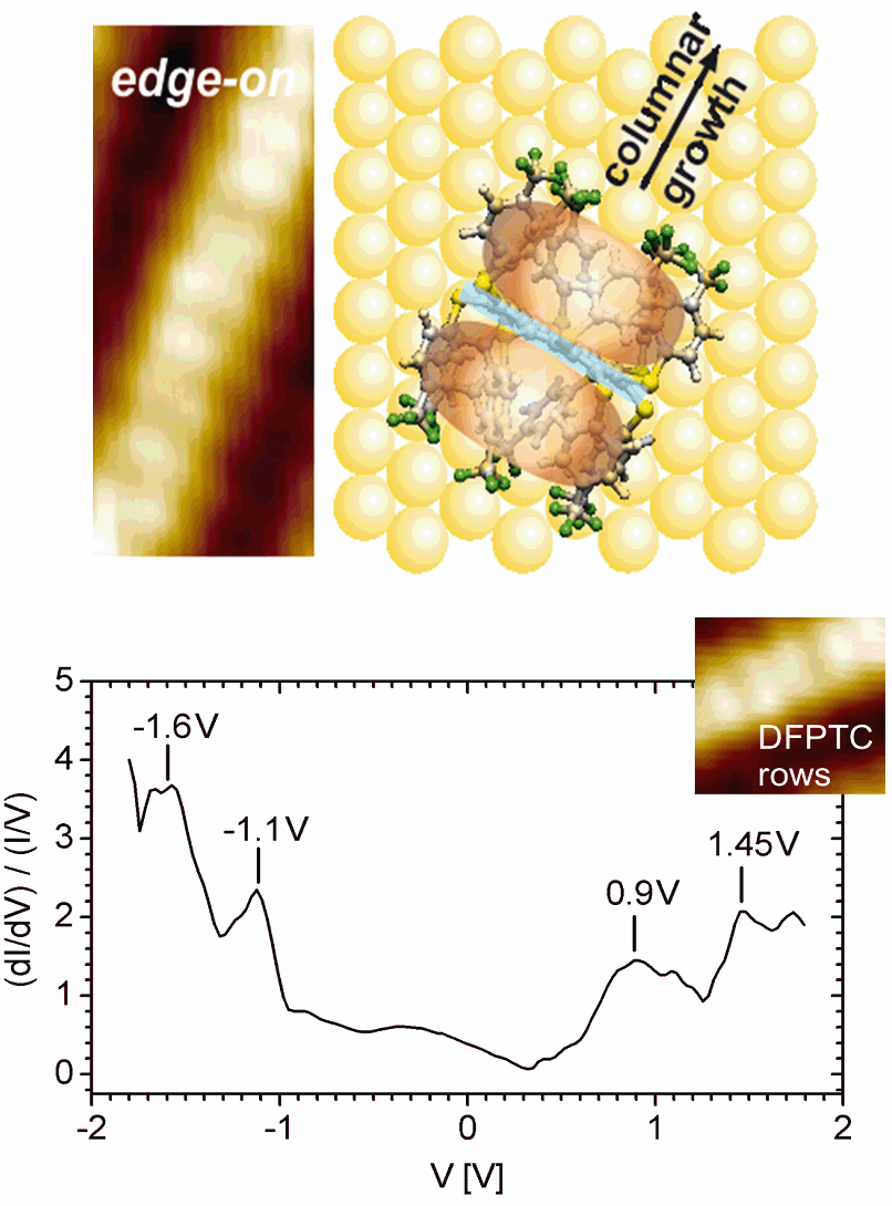
Figure 1: (a) STM image and corresponding schematic of a DFPTC columnar structure on Au(111). The molecules are observed to form supramolecular columns along the [11-2] direction of the underlying gold surface. The distance between bright intracolumnar features has the average value aSTM = (0.47 ± 0.05) nm. (b) STS characteristics measured on top of the columnar DFPTC structure.
To gain insight into the detailed molecular structure and possible intermolecular interactions, respectively, we performed DFT calculations including long range van der Waals (vdW) interactions. In the first instance, we investigated the geometrical structure and the stability of several conformers of the isolated single molecules. Three different stable conformations were obtained (Fig. 2): (i) in the up-down conformer adjacent aryl groups alternate between the position above and below the plane of the coronene unit, (ii) in the 2up-2down conformer alternately two adjacent aryl groups are located above and below the plane, and (iii) in the up-up conformer all 12 aryl groups are located above the coronene plane. The ab initio calculations reveal that the up-up conformer of all investigated DPTCs is significantly less stable than the other two conformers (Table 1). This suggests that the columnar structures should consist of molecules having a conformation with an alternating pattern of the substituents above and below the coronene core, that is a conformation close to up-down or 2up-2down. During the aggregation into the columnar structure, a geometrical reorganization of the peripheral groups is expected to occur and enable a commensurable growth on the Au(111) surface.
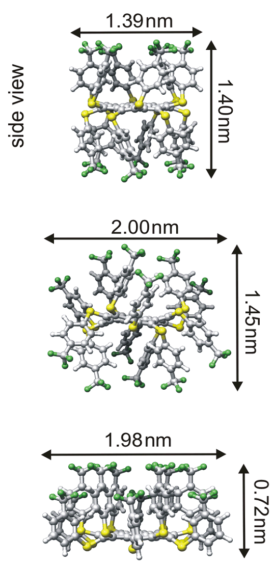
Figure 2: Top and side views of the optimized geometries of the DFPTC conformers: (a) up-down, (b) 2up-2down, and (c) up-up conformer.
|
| up-down
| 2up-2down
| up-up
|
| DFPTC | +0.16 | 0 | +0.77 |
| DPTC | 0 | +0.19 | +0.68 |
| DMPTC | 0 | +1.15 | +1.18 |
Table 1: Total energies in eV of DPTC conformers. (The total energy of the most stable conformer is set to the reference value 0 eV for all three DPTC molecules.)
Comparing experimental and theoretical results several important statements should be noted: (i) The topographic appearance and the corresponding energy gap of single DFPTC molecules within the disordered layer fits best to the DFT results of the up-down conformer. (ii) DFPTC molecules with a threefold symmetric appearance can be assigned to the 2up-2down conformer since the experimentally measured intramolecular features and the energy gap fit almost perfectly to the theoretical values [1]. (iii) STS of DFPTCs within the columnar structure exhibit distinctly different features when compared to the characteristics of single non-aggregated molecules. The observed set of HOMO/LUMO levels is explained by the overlap between the peripheral groups within the DFPTC columns which should enable charge delocalization and thus lead to the build up of one-dimensional charge transport channels.
An opposed behaviour is observed in the case of the DMPTC molecules adsorbed face-on on Au(111) (Fig. 3). The impact of the methoxy-functionalization is twofold. Firstly, these groups seem to anticipate a stacking of the molecules and, secondly, they point towards the surface and therewith act as distance defining (insulating) spacers giving rise to a tunneling barrier between the substrate and the three-dimensional aromatic/delocalized electronic system of the molecules (Fig. 3). A double-barrier tunnel junction is formed in this way and leads to the occurrence of single electron tunnelling effects in STS measurements.
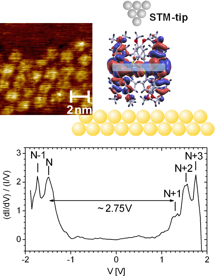
Figure 3:
(upper part) STM image of DMPTC molecules and a sketch showing that the methoxy groups pointing towards the substrate act as spacers, giving rise to an additional tunnelling barrier between the substrate and the three-dimensional aromatic system of DMPTC.
(lower part) STS data of DMPTC adsorbed on Au(111) in face-on configuration showing peaks related to subsequent charge states of the molecule.
We conclude that by using systematically substituted phenylthio-moieties the self-assembly behaviour of DPTC-derivatives was directed into different regimes. Thus the tendency to form columnar structures of molecules in edge-on configuration was strongly enhanced when using electron-with-drawing CF3 substituents (DFPTC). The face-on adsorption of DMPTC together with not fully delocalized molecular orbitals, on the other hand, is accompanied by an electronic decoupling of the aromatic system from the substrate. This goes along with the creation of a double-barrier tunnel junction configuration and the occurrence of single electron transport features visible in the tunnelling spectroscopy. In conclusion, the investigated DPTC system can be tailored in such a way that quite different advantageous electronic functionalities are achieved.
- [1] P. Kowalzik, N. Atodiresei, M. Gingras, V. Caciuc, N. Schnaebele, J.-M. Raimundo, S. Blügel, R. Waser, and S. Karthäuser, Phys. Chem. Chem. Phys. 14, 1635-1641 (2012).
- [2] P. Kowalzik, S. Rathgeber, S. Karthäuser, R. Waser, N. Schnaebele, J.-M. Raimundo and M. Gingras, New J. Chem. 36, 477-483 (2012).
- [3] P. Kowalzik, N. Atodiresei, M. Gingras, V. Caciuc, S. Blügel, R. Waser, and S. Karthäuser, J. Phys. Chem C 115, 9204-9209 (2011).
Peter Kowalzik, Nicolae Atodiresei1, Vasile Caciuc1, Stefan Blügel1, Marc Gingras2, Rainer Waser, and Silvia Karthäuser
1Peter Grünberg Institut-1
2CNRS, Aix-Marseille University, UPR 3118 CINAM, 13288 Marseille Cedex 09, France
Electrical Transport Through Single Nanoparticles and Nanoparticle Arrays
Electrical transport measurements on 3D arrays as well as on individual particles were performed on biphenylpropanethiol-capped gold nanoparticles with a diameter of 4 nm. The individual nanoparticle measurements exhibit Coulomb blockade behavior at room temperature. Depending on temperature different types of transport mechanisms can be distinguished, such as hopping, superexchange coupling, and tunneling. Furthermore, a discontinuity in the temperature dependent conductance was observed between 200 and 290 K. This discontinuity might be a consequence of a theoretically predicted structural crossover in the particle´s morphologies.
Due to their unique electrical properties and their ease of modification ligand stabilized gold nanoparticles (AuNPs) are interesting building blocks for nanoelectronic applications. However, application of such nanoelements requires detailed investigations of the charge transport characteristics in order to understand and control the electrical transport. In this context we have synthesized biphenylpropanethiol (BP3)-capped AuNPs and performed detailed studies on the charge transport through BP3 capped AuNP arrays as well as through individual AuNPs. The particles have been synthesized in a two phase approach[1]. TEM measurements revealed particles with narrow size distribution and a mean metal core diameter of 4.1 ± 0.5 nm (derived from 251 particles).
Arrays of BP3 capped AuNPs were formed on IDE structures (interdigitated electrode structures) by drop casting a solution of AuNPs in toluene. The electrical transport characteristics were investigated by complex impedance measurements, recorded as a function of frequency (10 mHz - 1 MHz) and temperature (340 > T/K > 10) at a constant voltage (USD = 100 mV). The results are depicted in Figure 1. In principle, depending on temperature three different transport regimes can be distinguished. The first and the third regime (Fig. 1, (I) Tred = 300–340 K, EA = 184 meV; (III) Tblue = 100–220 K, EA = 58 meV), follow a linear dependence according to the Arrhenius relation. For regime (I) a hopping process between nearest neighbors is deduced, while in regime (III) the charge transport is less temperature dependent and resembles features of the granular metal model or the superexchange model, respectively. However, in the second regime (Fig. 1, II) Tyellow = 230–290 K) an atypical discontinuity is observed. An explanation might be a transition in the particle morphologies, which has been proposed from relativistic ab initio calculations [2].
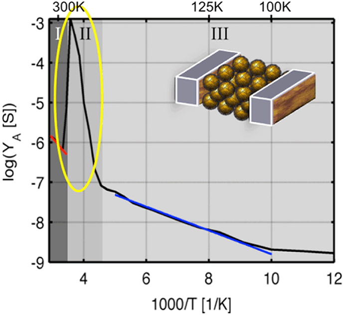
Figure 1: Temperature-dependent conductance of a BP3-AuNP array plotted according to Arrhenius (log YA vs T-1). The yellow circle marks the discontinuity in the I-V characteristic.
In order to investigate the charge transport on individual BP3-capped AuNPs, tailored nanoelectrode configurations have been prepared by e-beam lithography. A new fabrication route based on an optimized two-layer resist system in combination with an adopted developer system, as well as an elaborated nanoelectrode pattern was developed in order to achieve reproducible nanoelectrode structures comprising sub-5 nm gaps (Fig. 2) [4].
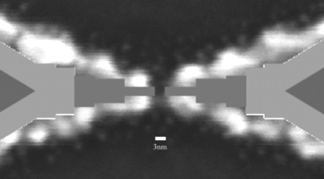
Figure 2: High resolution SEM of nanoelectrode pairs with electrode separation of 3 ± 1 nm and a fabrication yield of 55% [4].
Immobilization of BP3-AuNPs was performed by dc dielectrophoretic trapping (DC-DEPT). Electrical measurements on the individual nanoparticle-nanogap test-devices were performed in a continuous flow cryostat with varying temperature (RT-4 K). It should be noted that the resistances measured for empty nanoelectrode gaps are usually larger than 1 TΩ, while nanoelectrode gaps filled with BP3-AuNPs exhibit resistances smaller than 10 GΩ. The temperature-dependent conductance obtained for the nanoelectrode/BP3-NP—BP3/nanoelectrode device is depicted in Fig. 3.
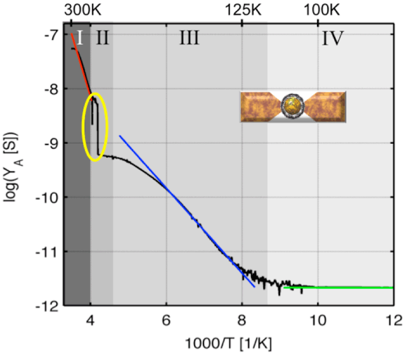
Figure 3: Temperature-dependent conductance of an individual BP3-AuNP plotted according to Arrhenius (log YA vs T-1). The yellow circle marks the significant singularity in conductance at T ∼ 235 K.
Four different transport regimes can be distinguished clearly and are attributed according to their temperature dependence, to different transport mechanisms. In the highest temperature range (Fig. 3, (I), Tred = 265–245 K) an exponential decrease of the conductivity with decreasing temperature is observed, which is assigned to a thermally activated charge transport reflecting an activated hopping involving molecular moieties. In the lower temperature ranges (Fig. 3, (III), Tblue = 200–110 K and (IV), Tgreen < 110 K) a weaker temperature dependence or no significant temperature dependence are observed, respectively. In the temperature range Tblue superexchange coupling or electrical transport according to the granular metal model is considered as underlying charge transport mechanism. The main conduction mechanism in the lowest temperature regime, Tgreen, corresponds to tunneling, either direct or Fowler–Nordheim tunneling. Significantly, an analogous discontinuity as observed for the arrays (Fig. 1, (II), Tdis = 230–290 K) can be detected for individual AuNPs (Fig. 3, (II), Tdis ∼ 235 K). Furthermore, this change of current, in the order of one magnitude, was fully reproducible, so that an accidental geometrical change can be excluded and thus might be referred to a transition in the particle morphologies.
Beside temperature dependent conductance measurements, we also performed cyclic I-U measurements of single BP3-AuNPs. Figure 4 depicts the resulting differential conductivity, (dI/dU), obtained from 250 cycles [4].
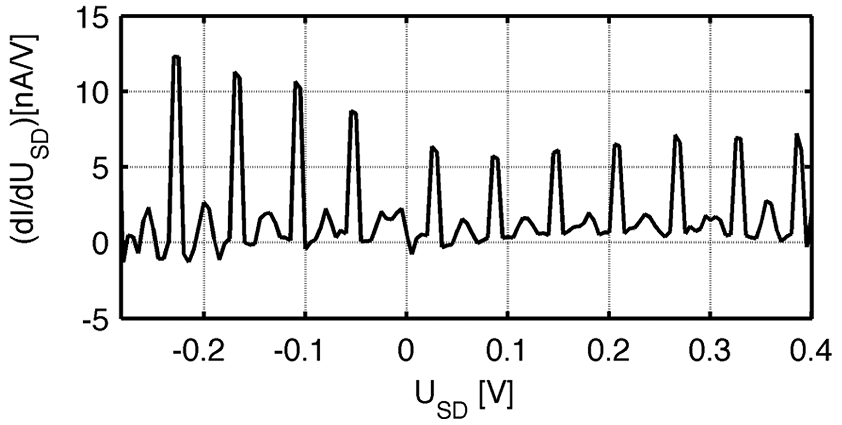
Figure 4: First derivative of cyclic I-U measurements on a single BP3-NP in a nanogap at RT (averaged over 250 cycles and flattened). Periodic peaks with a distance of ΔUCB = 61 mV and a height of ΔG ≈ 8 nS are detected.
Most interestingly, equidistant periodic peaks are measured over a large range of applied voltage, which can be attributed to Coulomb blockade peaks and indicate that the electrical current flows through a single NP only. The peak distances allow the determination of the charging energy (ΔUCB = 4EC/e; EC = 15 meV) and the total capacitance of the NP (EC = e2/2Ctot; Ctot = 5.2 aF). However, since EC > kBT = 25 meV is a necessary requirement for measurements in the “strong” Coulomb blockade regime, it is not surprising that Coulomb blockade peaks appear here only as small modification of the total conductance Nevertheless, the detection of Coulomb blockade behavior observable on a single-nanoparticle (NP) device at room temperature (RT) was so far only achieved in measurements with STM configurations and on AuNPs with a diameter of d < 2.0 nm [5,6]
Summarizing, the temperature dependent electronic transport investigations of BP3-AuNP arrays or individual BP3-AuNP revealed different transport mechanisms, assigned to thermally activated hopping, superexchange coupling, and tunneling. Furthermore, a discontinuity in the temperature dependence of the conductance in both experimental setups was observed, probably arising from a transition in the nanoparticle´s core morphology. Moreover, Coulomb blockade behavior was observed in the single-NP device at room temperature.
This work is supported by the DFG program Si609/9-1 and KA 1819/2-1.
- [1] M. J. Hostetler, et al., Langmuir 1998, 14, 17?30.
- [2] A. Barnard, et al., ACS Nano 2009, 3, 1431?1436.
- [3] M. Manheller, et al., J. Phys. Chem. C, 2012, 116, 20657-20665.
- [4] M. Manheller, et al., Nanotechnology 2012 23 (12),125302 (6pp).
- [5] R. P. Andres, et al., Science 1996, 272, 1323?1325.
- [6] U. Zhang, et al., Nano Lett. 2003, 3, 305?307.
Silvia Karthäuser, Marcel Manheller, Rainer Waser, Kerstin Blech1, and Ulrich Simon1
1Institute of Inorganic Chemistry, RWTH Aachen University
Electron Transport and Molecular Structure of Self-assembled Monolayers of Biphenylthiols
The structures and the electron transport properties of self-assembled monolayers (SAMs) of 4´‑methyl‑1, 1´‑biphenyl‑4‑alkanethiols (BPn) are studied by UHV-STM. Using asymmetric tunnel junctions, W(tip)/BPn-SAM/Au(substrate), the dependence of the tunneling current on the tip-substrate distance (IS-spectroscopy) has been obtained for BPn-SAMs with different alkane chain length (n = 2, 3, 5). From these data the decay constant of biphenyls is extracted. Furthermore, mixed SAMs have been formed by insertion of 4´‑methyl‑1, 1´‑biphenyl‑4‑butane (BP4) into a dodecanethiol (C12) SAM. Insertion preferentially takes place at domain boundaries or etch pits in the gold surface that are characteristic for C12 monolayers on gold. With a lower probability insertion also occurs inside dodecanethiol domains resulting in isolated BP4 molecules.
Thiol based self-assembled monolayers (SAMs) of organic molecules are an effective tool to tailor the surface properties of metals [1]. The applications of SAMs range from wetting control, corrosion inhibition, protein adsorption, and patterning to molecular electronics. Due to their potential applications, SAMs of alkanethiols have been intensively studied in recent years [2–4]. Besides alkanethiols, aromatic thiols such as biphenyl-alkanethiols have moved into the focus of current research interest [5, 6]. These molecules are supposed to show more interesting electron transport properties than simple aliphatic thiols due to the conjugation along the aromatic backbone. To understand how an aromatic headgroup influences the structure and the electron transport properties of the formed SAMs, we focus our investigations on 4´‑methyl‑1, 1´‑biphenyl‑4‑alkanethiols (BPn). A careful control of the BPn-SAM structure down to molecular dimensions is a prerequisite to perform electron transport studies through single molecules by current-distance spectroscopy (IS).
Single component SAMs of BPn´s have been grown from ethanolic solutions on (111)-oriented Au thin-films on mica [7]. Mixed SAMs of BP4 and dodecanethiol (C12) have been obtained by a two step deposition process, which is mainly used for insulating electrically active molecules in a host matrix. This method starts from a preassembled close packed SAM consisting of insulating alkanethiols which is dipped in a second step into a solution of the electronically active molecules. Structural investigations and scanning tunneling spectroscopy were performed with a JEOL JSPM 4500 UHV-STM with a base pressure of 3 × 10⁻¹⁰ mbar.
SAMs of 4´‑methyl‑1, 1´‑biphenyl‑4‑alkanethiols display a distinct odd-even effect [5, 6]. While BPn with n = 3.5 show a very well defined (2√3 × √3) structure with the sulfur-headgroups forming a √3 × √3 structure adopted to the (111)-Au lattice like alkanethiols, this is not possible for BPn with n = even. Their biphenyl unit is forced in a considerably more tilted conformation due to the even number of CH2 units in the alkane chain. This results in an enlarged area per molecule and consequently the molecules do not fit to the periodicity of the Au-lattice. Whereas for BPn, n = odd, a low energy structure in terms of molecular conformation, Au-S-C bond angle and adsorption sites on the gold lattice can be obtained, for BPn, n = even, this configuration is not possible. The obtained structure (Figure 1) is determined by an interplay between the forces acting on the molecule, as the molecule-substrate interaction, the intermolecular interactions and the forces due to conformational energies.
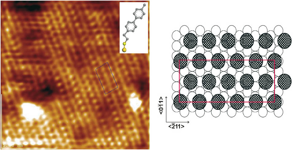
Figure 1: Left side: 14 × 14 nm2 scan of the low density structure of BP2 (inset) with an area per molecule of 0.36 nm2; right side: schema of the (4 × 6√3) unit cell.
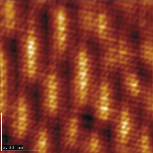
Figure 2: Systematic height modulation caused by structural mismatch between BP2 and gold lattice (scan size 20 × 20 nm2.
When BP2 is deposited at T = 90 °C ordered domains of large size result. They exhibit small, periodic height variations on the length scale of several nanometers. The reason for this superstructure is the structural mismatch between the molecular adlayer and the gold substrate, which results in this long range modulation (Figure 2).
Besides the structural characterization, monolayers of BPn have been also studied by IS spectroscopy. The BPn-SAM is shown to be composed of two parts, which are identified by different decay constants β (Figure 3). These parts are interpreted as the biphenyl unit and the alkane chain of BPn. By these IS-measurements, the decay constant β of the biphenyl unit is determined to be 4.7 nm–1.
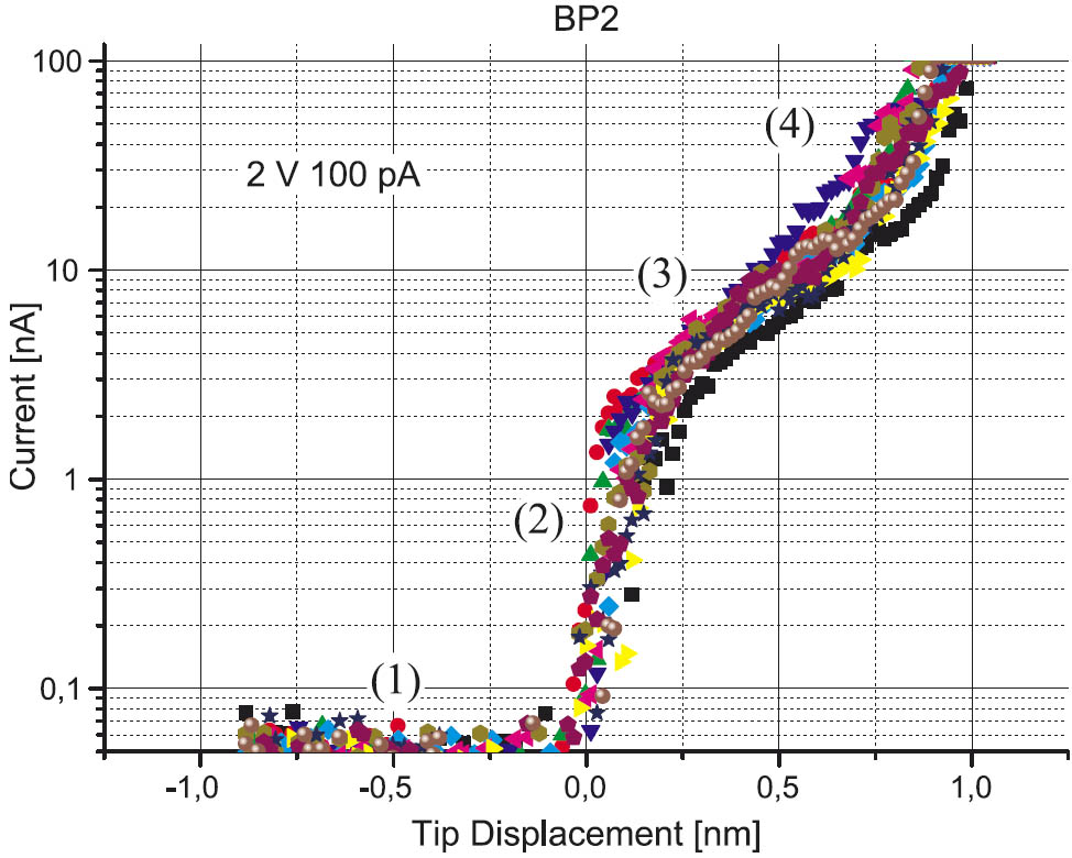
Figure 3: Current-distance curves (IS) for BP2 exhibiting four different tunneling regimes: no tunneling current at large tip-substrate distances (1), tunneling current increasing with large gradient in vacuum (2), tunneling regime attributed to the biphenyl-moiety (3) and to the alkane chain (4), respectively.
Mixed SAMs have been obtained by insertion of BP4 into a close packed SAM of C12 on Au(111). Insertion takes place at defect sites such as domain boundaries or etch pits in the gold surface that are characteristic for C12 monolayers on gold. With a lower probability, insertion also occurs inside C12 domains, which are molecularly resolved (Figure 4). Insertion at defect sites results in domains of BP4, whereas insertion into C12 domains leads to isolated BP4 molecules [8]. The isolated BP4 molecules are shown not to move at room temperature. By comparing the apparent height of the isolated BP4 molecules and BP4 domains it is proposed that the isolated molecules have the same conformation as in the full coverage phase.
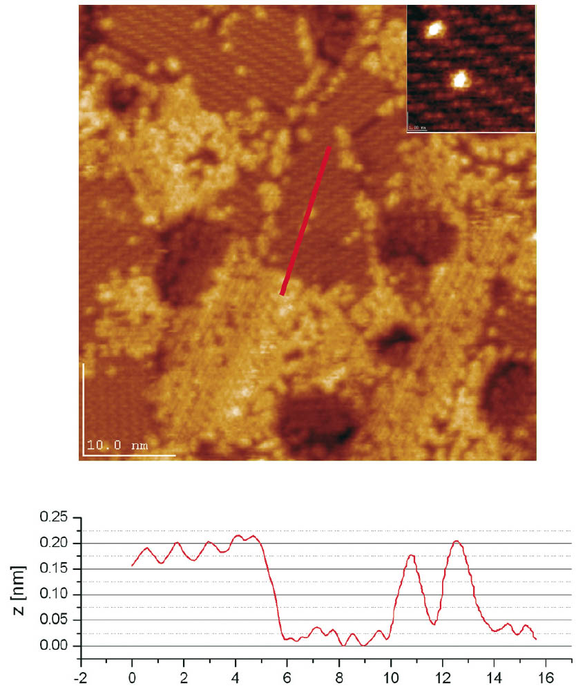
Figure 4: Upper part: 50 × 50 nm2 STM scan of the mixed BP4/C12 monolayer. Inset: zoom of single BP4 molecules inserted into a C12 domain (6 × 6 nm2). Lower part: cross section along the red line in the upper image. [8].
Figure 4 also shows a zoom of an area, in which BP4 molecules appearing as protrusions are inserted into a C12 domain. Also visible is the (3 × 2√3) structure of the underlying C12 monolayer which provides a coordinate system to measure the lateral dimensions of the embedded molecules. All protrusions have the same lateral size and appear to be smaller than one unit cell of C12, which consists of four C12 molecules. Considering the relatively larger occupied area per molecule for BP4 compared to C12 and that the STM image is a convolution of the imperfect STM tip shape and surface geometry, we propose that these protrusions consist of only single molecules.
In this report we demonstrated molecularly resolved UHV-STM images of biphenyl-alkanethiol SAMs und deduced the decay constant for phenylene-groups from IS-measurements. Furthermore biphenyl-alkanethiols have been inserted into an insulating alkanethiol host-matrix leading to BP4 domains and single insulated BP4 molecules. Especially this latter method bears the potential for the characterization of electron transport properties through single functional molecules.
- [1] F. Schreiber, Prog. Surf. Sci., 65, 151 (2000).
- [2] J. C. Love, L. A. Estroff, J. K. Kriebel, R. G. Nuzzo, G. M. Whitesides, Cem. Rev. 105, 1103–1169 (2005).
- [3] B. Lüssem, L. Müller-Meskamp, S. Karthäuser, and R. Waser, Langmuir 21, 5256 (2005).
- [4] L. Müller-Meskamp, B. Lüssem, S. Karthäuser, and R. Waser, J. Phys. Chem. B 109, 11424 (2005).
- [5] H.-T. Rong, et al. Langmuir 17, 1582 (2001).
- [6] P. Cyganik, M. Buck, W. Azzam, and Ch. Wöll, J. Phys. Chem. B. 108, 4989 (2004).
- [7] B. Lüssem, S. Karthäuser, H. Haselier, and R. Waser, Applied Surface Science 249, 197 (2005).
- [8] B. Lüssem, L. Müller-Meskamp, S. Karthäuser, M. Homberger, U. Simon, and R. Waser, Langmuir, accepted.
B. Lüssem, S. Karthäuser, R. Waser
Self-Assembly of Mixed Monolayers of Mercaptoalkylferrocenes for Nanoscale Surface Patterning
The self-assembly behaviour of a series of mercaptoalkylferrocenes embedded into ordered alkanethiol monolayers from solution is studied. Upon annealing, the inserted ferrocene derivatives form separated domains, which protrude as islands from the surrounding monolayer. The resulting thin films are characterized by UHV-STM and the density and the structure of the close-packed self-assembled monolayers is determined. Besides this the molecular structures of submonolayer phases of ferrocenes in mixed layers with alkanethiols are identified. The ferrocenes form a striped surface phase resulting in equispaced rows of ferrocene moieties. The obtained nanoscale lattice of functional groups offers interesting options for patterning of small, periodic surface structures with precise distance control via hydrocarbon spacers.
The fascinating power of molecular self-assembly is a promising tool for a possible integration of non-silicon technology into nanoelectronic devices [1]. A particularly well characterized system of self-assembled monolayers (SAM) is the system of alkanethiols on Au(111) substrates. These monolayers can be used to embed functional molecules into a mechanically stable and electrically insulating environment to study their electrical properties [2]. Especially interesting for future technological applications is the insertion of electroactive molecules like mercaptoalkylferrocenes. These molecules can be easily oxidized and reduced in solution and are well characterized by electrochemical methods [3], although the mercaptoalkylferrocenes tend to aggregate and form multilayers [4]. Therefore, to achieve stable layers with better defined properties, we inserted the mercaptoalkylferrocenes into SAMs of alkanethiols with an accordant molecular length and studied the structural properties of the mixed monolayers by UHV-STM [5–7].
Mixed monolayers of mercaptoalkylferrocenes and alkanethiols were assembled in a two step deposition process from ethanolic solutions onto crystalline, (111)-oriented Au thin-films on mica. This method starts from a preassembled close packed SAM consisting of insulating alkanethiols which is dipped in a second step into a solution of the electronically active molecules. During this step a moderate heating is performed to improve the quality of the monolayer. Structural investigations and scanning tunnelling spectroscopy were performed with a JEOL 4500 UHV-STM at a base pressure of 1 × 10⁻¹⁰ mbar.
The thus insertion processed, mixed monolayers of 1,1”-dithiobis-ferrocene (Fc) and octanethiol (C8) show two domain types differing in their surface structure (Figure 1). One displays the characteristic surface structure of an octanethiol SAM with a striped/lying-down phase while the second domain type, formed during insertion and annealing, consists of ferrocenes. From the homogenous height of the Fc-island a layer thickness of exactly one monolayer can be deduced. Autocorrelation of the Fc-island structure shows a weak hexagonal order and an average distance of 0.67 nm between the centres of two nearest neighbours. Assuming that the Fc’s can be considered as small spheres in a hexagonal arrangement, an average surface area of 0.39 nm2 per molecule is calculated. This phase separation, already taking place at moderate annealing conditions, indicates a high mobility of the embedded Fc’s and a lower tendency for ferrocene-alkanethiol intermolecular interaction.
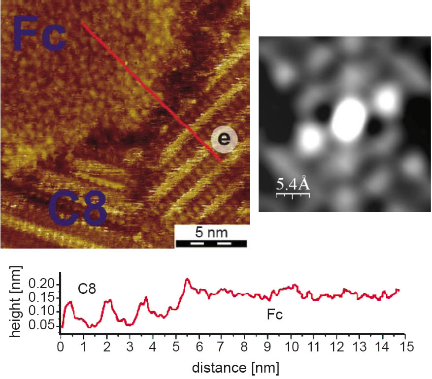
Figure 1: 1,1”-dithiobis-ferrocene (Fc) inserted into an octanethiol (C8) monolayer, showing the characteristically striped structure of lying-down alkanethiols and the disordered texture of the Fc-domain (left upper part). Upper right part: The self-correlation of the Fc-island structure indicates a loose hexagonal order. Lower part: profile of the octanethiol monolayer (C8) and the Fc-monolayer (Fc).
Analogous to the insertion of the Fc-molecules mercaptoalkylferrocenes with various alkane spacer chains were inserted into an undecanethiol-monolayer (C11). The mixed layers show the highly ordered SAM structure of alkanethiols and small islands of the ferrocene-derivatives with a crystalline order and a surface structure of elongated shapes, assumed as single ferrocene moieties (Figure 2). The resulting area of 0.7 nm2 per molecule seems reasonable, compared to 0.39 nm2 for Fc. An obvious feature of the ordered islands is the pairing of the ferrocene end-groups on the surface and since each ferrocene moiety of Fc(OC11)2 is associated with two alkane spacer-chains, the four alkanethiol chains are identified to be in the same arrangement as in a c(4 × 2) unit cell. Besides the phase separated islands a number of spots is observed, indicating the existence of individual ferrocenes in the C11 monolayer. This hindered interdiffusion is attributed to the intermolecular interaction between the alkane chains of the ferrocene derivatives and the host matrix.
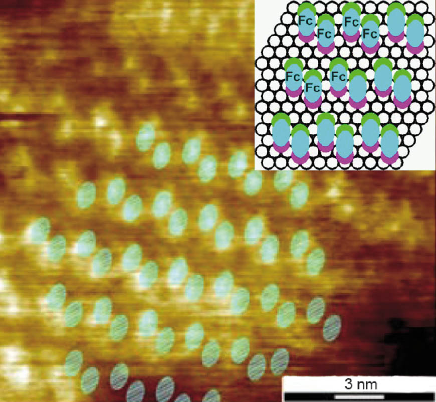
Figure 2: Crystalline domain of bis-mercaptoundecanoyl-ferrocene (Fc(OC11)2) embedded into an undecanethiol SAM (C11) and the schematic of the suggested placement for the Fc(OC11)2 molecules with respect to the gold lattice (inset). The green and pink dots represent the chemisorbed spacer groups, the bright blue ovals the associated ferrocene moiety.
For layers deposited from mixed solutions with a long insertion step at elevated temperatures, partially desorbed structures are found. In difference to the layers compared so far, the alkanethiols as well as the ferrocene derivatives are flat-lying on the surface, forming striped domains with varying orientations and line spacings. Diverse striped structures can be distinguished which differ in texture between the prominent rows, pointing out different phases and defects, as shown in Figure 3. The double row structures appear frequently on the surface and show line spacings dependent on the ferrocene derivative incorporated. From comparison of the height profiles for alkanethiols and mercaptoalkylferrocenes a replacement of alkanethiols by mercaptoalkylferrocenes is deduced with the thiol headgroup and the alkane spacer of the ferrocene compounds being positioned in the same way as in a striped alkanethiol phase. The ferrocene endgroups point to the center, forming a double row, and the thiol headgroups build bright pairs with the next row.
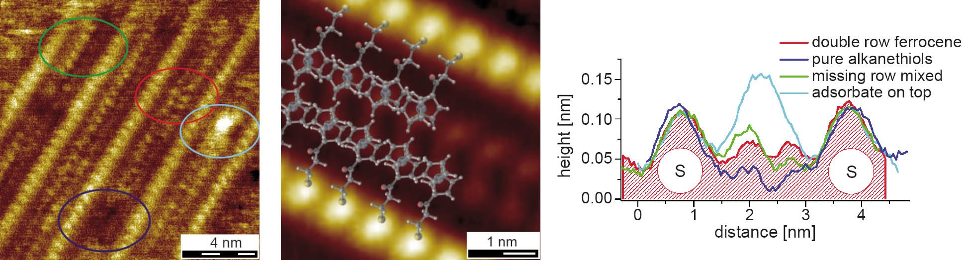
Figure 3: On the left a view of the different striped structures observed for mercaptopropanoyl-ferrocene (FcOC3) is shown. The dark blue circle marks a missing central feature, the red one a double row, the green a single row, and the light blue additional adsorbates. In the middle a filtered STM scan of the lying-down, double row structure with the assumed molecular arrangement is given. On the right, the profiles of the different structural variations of the lying-down phases marked in the left image are displayed.
In this report real space structural information of chemisorbed ferrocenes inserted into alkanethiol monolayers is given. For ferrocenes without spacer-chains, a strong tendency for phase separation and only slightly ordered structures are found, while crystalline domains are observed for ferrocenes with longer spacer chains. For lower coverage an interesting structure of lying-down ferrocenes and alkanethiols forming nanoscale pattern is obtained, whose period is shown to be defined by the length of the lying-down molecule. Thus the period of the structure can be controlled by the alkane spacer length, while the functionality of the ferrocene endgroup is still accessible. It can be concluded that in general it will be possible to generate striped surface structures with adjustable distances and desired chemical functionalities by systematic modification of an alkanethiol spacer and by using a customized endgroup.
- [1] M. Homberger, S. Karthäuser, U. Simon, B. Voigtländer, “Formation of Nanostructures by Self-Assembly” in “Information Technology” ed. by R. Waser, Wiley (2008)
- [2] Z. Donhauser et al., Science 292, 2303–2307 (2001)
- [3] C. Chidsey, C. Bertozzi, T. Putvinski, A. Mujsce, J. Am. Chem. Soc. 112, 4301–4306 (1990)
- [4] A. Viana, L. Abrantes, G. Jin, S. Floate, R. Nichols, M. Kalaji, Phys. Chem. Chem. Phys. 3, 3411–3419 (2001)
- [5] L. Müller-Meskamp, B. Lüssem, S. Karthäuser, S. Prikhodovski, M. Homberger, U. Simon, R. Waser, Phys. Stat. Sol. 203, 1448–1452 (2006)
- [6] L. Müller-Meskamp, B. Lüssem, S. Karthäuser, M. Homberger, U. Simon, R. Waser, J. Phys. Conf. Ser. 61, 852 (2007)
- [7] L. Müller-Meskamp, S. Karthäuser, R. Waser, M. Homberger, U. Simon, Langmuir accepted
S. Karthäuser, L. Müller-Meskamp, M. Homberger1, U. Simon1, R. Waser
1Institute of Inorganic Chemistry, RWTH Aachen University, Germany