electrochemistry at the nano scale

In electrochemical processes, the size reduction of structures from the micrometer to the nanometer scale leads not only to a miniaturization of fabricated or modified units, improved cells for e.g. photolytic hydrogen production but also has tremendous fundamental implications. Processes at the nano scale typically take place below dimension of the space charge regions in solid electrolytes or the diffusive double layer in liquid electrolytes, so that the requirement of an overall charge neutrality can be dropped and new degrees of freedom are opened. We are interested in electrochemical metal deposition and metal dissolution reactions at the scale of few nanometers for non-volatile resistive switching memories which show the potential of intergration densities up to the Terabits per sqcm range - similar as the oxide based redox systems. In addition, we use electrochemical processes at the fabricate nano gap for complex molecules which are interesting because of their electronic functions. In this context we also pursue a research activity in the area of photoelectrochemical cells and photocatalytical H2 generation systems.
Electrochemistry at the Atomic Scale – Nucleation, Charge Transfer and Imaging
The ability to control at the atomic scale the physicochemical properties of surfaces is of primary interest for a wide range of fields, including energy conversion, nanoelectronics and information technology, and nanoionics.
Electrochemically formed new phase consisting of a few to some tens of atoms in contact with foreign substrate is expected to be thermodynamically instable (as far it can be physically defined as a phase). The charge, transferred in the elementary act(s) cannot exceed these tens of e− which is beyond the sensitivity limits of modern instrumentation. An uncertainty is additionally introduced by the fact that the well defined macroscopic quantities are averaged and even single crystalline substrates show local structural defects leading to microscopic inhomogeneities of the material properties. Therefore, the atomically resolved measurements of electrochemical processes require: i) a high precision in detecting mass and charge flow, ii) a stabilisation of thermodynamically meta-stable clusters of few atoms and iii) a knowledge of the local atomic structure and topography.
Atomically resoved STM imaging
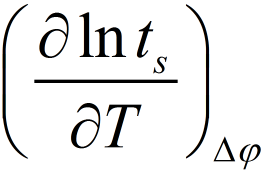
We succeeded to provide for the first time atomically resolved STM images of superionic solid electrolyte by small amount of Fe-doping which increases the electronic partial conductivity of RbAg4I5 and allows quantum mechanical tunnelling.
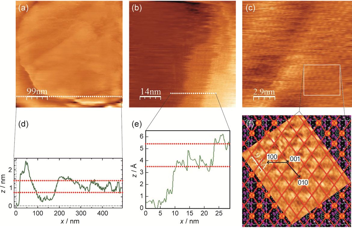
Figure 1: STM images of a RbAg4I5 grain (a), and monatomic steps (b) with the corresponding (x-z) profiles (d),(e). Atomically resolved (110) face is shown in (c) and (f). The brighter spots display the I− ions. The images were recorded using a set point tunnelling current of 1 nA at tunnelling voltages of 50 mV, 75 mV and 75 mV for images (a), (b) and (c), respectively (below the decomposition voltage of RbAg4I5).[1]
Atomically resolved electrochemical kinetics
The initial stages of Ag cluster formation were studied by applying a negative voltage to the STM tip fulfilling the condition EF(tip) + eΔφ > EF(Ag+/Ag). Due to the specifics of the system no steady state measurements can be performed but rather short voltage pulse experiments. Applying a negative voltage pulse, a switching event occurs (short circuiting the vacuum gap [2]) in times ranging between some ms and ns, with switching times ts being exponentially dependent on the value of the applied potential.
Figure 2: Current-time dependence at applied voltage of −100 mV. ti (i = 1–5) denotes the starting time of the ith process step. The number (1–5) notation relates the 5 regions defined in the current-time characteristics to the microscopic model (upper part of the graph) for the sequence of individual physicochemical processes during the switching. Only 4 Ag atoms in a chain are sufficient to short circuit a gap of 1 nm (typical tip-sample distance). Accounting for dispersion of the tunnelling current beam area up to 20 Ag atoms can be calculated to constitute a cluster of a conical or tetrahedral form. The inset shows the first quantum step at G0. The sharpness of the current increase is determined by the rate of the filament growth. [1]
The time for the growth process is given by tg. Figure 2 indicates that tg can be neglected and presuming tn ~ ts the relation between ts and is derived:
For cathodic voltages, Δφ takes negative values and the switching time decreases exponentially with increasing cathodic voltage.
Based on the applied voltage/time plots and their temperature dependence we extracted the kinetic parameters of the electrochemical reaction.
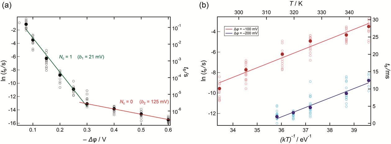
Figure 3: Dependence of the switching time ts (a) on the applied voltage for T = 300 K, and (b) on the temperature at two constant voltages. Because the nucleation is a stochastic event a statistical dispersion of ts values is expected. Every data point is extracted from an analysis such as the one shown in Figure 2. [1]
The two regions presented on Figure 3a correspond to different number of atoms required to form the critical nucleus.
Thus, in Region 1 we found Nc = 1 and in Region 2 Nc = 0. Nc = 1 has the physical meaning that each atom of Ag created at the RbAg4I5 surface can be considered as a nucleus of the new phase and Nc = 0 means that an empty nucleation site acts as a critical nucleus and the single created Ag atom represents a supercritical cluster of the new phase.
The activation energy of the nucleation process can be obtained from the temperature dependence of the switching time from the slope
In Figure 4b the results at constant voltages of −100 mV and −200 mV are shown. The mean activation energy was found to be ΔGa = (1.0 ± 0.1) eV. This result proves firstly, that the electrochemical barrier (nucleation) and not the tunnelling barrier controls the overall reaction rate and secondly, it definitely excludes the diffusion of Ag+ ions in the RbAg4I5 to be rate limiting, because this shows a very different value of approx. 0.12 eV. However, we should note that the determined energy barrier includes both terms - the charge transfer and the surface energy term given in the first pre-exponential factor of equation (1).
Nucleus imaging and stability
To image clusters by STM and determine their life time pulses of different amplitudes were applied with a switched on feedback modus. Thus, by fast withdrawing the tip, the clusters were not allowed to mechanically contact the STM tip (no switching event occurs). The deposited clusters (if stable) were imaged afterwards in a positive voltage regime.
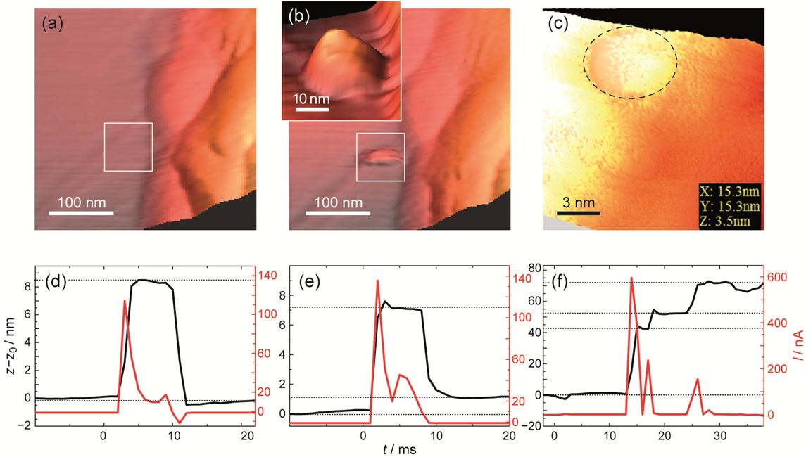
Figure 4: STM observations of Ag clusters formation and stability. 3D STM imaging of RbAg4I5 surface: (a) before applying a voltage pulse and (b) after the cluster is formed. In (c) the smallest filament we were able to detect is shown. Determination of the filament height by I-z measurements is shown in (d–f). In (d) the pulse length was 10 ms (Δφ = −250 mV); for (e) the pulse length was the same but Δφ = −350 mV and in (f) the pulse length was 50 ms and. z0 denotes the initial z-position. The change in the current is associated with a z-variation due to partial growth and dissolution of Ag (Itunnel depends exponentially from the tip-sample distance). [1]
No upper limit of the filament size was found but there is a lower size limit determined by the thermodynamic stability of the Ag phase. The smallest cluster we succeeded to detect by STM imaging was approximately 5 nm in diameter and 3 nm in height (Figure 5c). Stability of smaller clusters with a height of down to 1 nm was indicated by I - z measurements shown in Figure 5e. However, their long term stability could not be confirmed by imaging. Free standing clusters below this size were unstable. We detected their formation and life time only by I - z measurements. Figure 5d shows the current (z) oscillations during the formation and a complete dissolution of meta-stable clusters. After the end of the pulse, the current value equals to the value before the pulse i.e., no irreversible morphology change had occurred. For higher cathodic voltages the clusters can be stabilized and a step-wise growth can be observed (Figure 5e,f). Thus, we demonstrated for the first time free standing clusters and observed their dynamics.
I. Valov, R. Waser
Controlled Quantized Conductance in AgI Based Resistive Switches Highlights Opportunity for Atomic-Scale Memory
Resistive switches are considered to be a potential candidate to overcome the obstacles of current memory devices as they offer the prospect of ultimately high scalability. On the way towards future information technology we report on silver iodide (AgI) based resistive switches where we observed controllable quantize conductance of a nanosized metallic filament within a solid electrolyte, raising the prospect of an atomic-scale memory.
As the conventional charge based non-volatile Flash memory is expected to approach its downscaling limit within the next years, researchers are prospecting alternative concepts to overcome the obstacles of current information technology. Recently, high attention has been paid to the resistive switching random access memories (ReRAM) based on nano-ionic redox phenomena as potential candidates [1]. Within the context of ReRAMs electrochemical metallization cells (ECM) represent emerging memory devices due to their fast operation, prospect of scalability, low energy consumption, ease of fabrication and potential multibit storage.
The ECM cell arrangement as depicted in figure 1 consists of a nanoscale electrolyte material sandwiched between an electrochemically inert counter electrode (e.g. platinum) and a working electrode (e.g. silver). The resistance of the cell can be reversibly modulated between a high resistive state (HRS) and a low resistive state (LRS), depending on the voltage polarity of an applied voltage pulse. Hereby, the resistance transition is attributed to the electrochemical formation and rupture of a nanoscale metallic filament [2]. The HRS and LRS can be assigned to binary OFF and ON states. Quantized conductance values for the cell resistance have been observed only in "atomic switch" type memory with a vacuum gap between the electrolyte and the counter electrode [3]. However, for purely solid state electrolyte based ECM cells being highly attractive for practical use a similar behavior has not been reported yet.
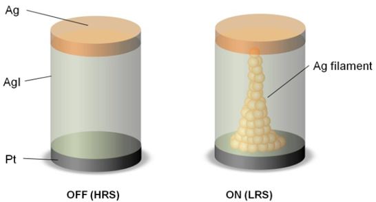
Figure 1: Schematic of a AgI based resistive switch in OFF state (HRS) and ON state (LRS). Formation and rupture of a metallic filament is believed to be responsible for resistance transition.
In this contribution we fabricated Pt/AgI/Ag micro crossbars with AgI electrolyte of thickness of 30 nm using conventional physical vapor deposition such as thermal evaporation and sputtering. Special attention has been paid to the pattern transfer since AgI is very sensitive towards chemicals (e.g. basic resist developer) and UV light which is needed for lithography. We employed an alternative pattern transfer process avoiding the impact of basic chemical and UV light demonstrating the prospect of downscaling to lateral dimensions of 100 nm and below.
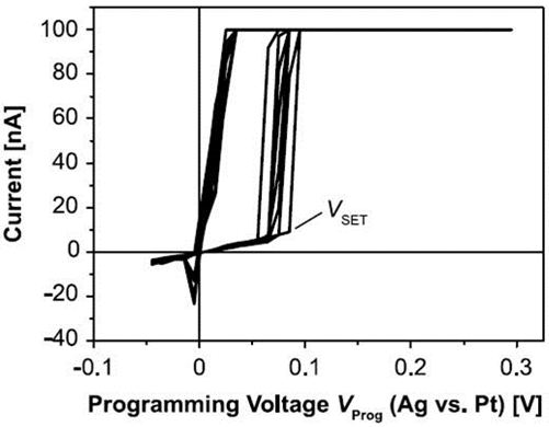
Figure 2: Resistive switching of AgI based micro crossbars. [4].
AgI micro-crossbars show reliable resistive switching characteristics (figure 2) and multibit storage can be achieved by varying the current compliance needed to prevent damage of the cell in the LRS during voltage sweeping [4].
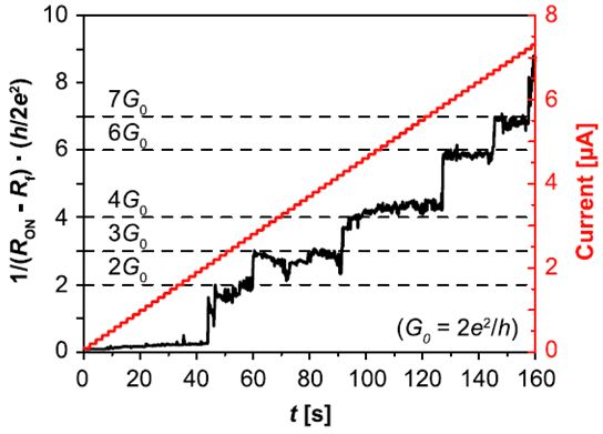
Figure 3: Quantized conductance values during current sweeping show that multiple of the single atomic point contact conductivity are dominating the cell resistance RON. For simplification, the filament resistance Rf is subtracted [4].
Similar switching characteristics have been lately reported for other material systems such as SiO2 [2]. We now successfully observed quantized resistances in LRS within a current window by current sweeping as shown in figure 3 [4].
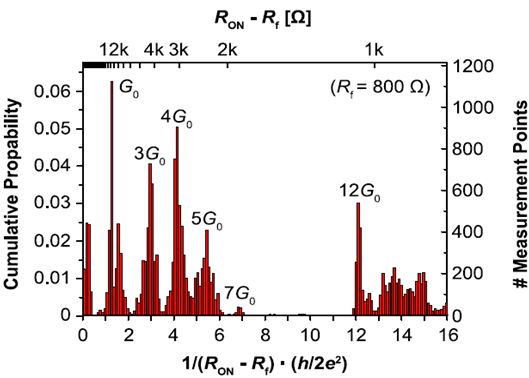
Figure 4: Cumulative statistics of controllable quantized conductance of AgI based memory cells [4].
These resistances imply the existence of quantized conductance higher than G0 = 78 µS which can be identified as multiple of the single atomic point contact conductivity. The switching behavior clearly indicates that the actual cell resistance is dominated by some few or just a single atom which highlights the potential of an ultimate atomic scale memory. By adjusting the current during current sweeping we were able to control the quantized cell conductance and thus the number of filament atoms being responsible for the cell resistance. This is further supported by a cumulative statistics depicted in figure 4.
In summary, we successfully observed a controllable quantized conductance of resistive switching AgI micro crossbars giving the prospect of an ultimate scalability of these memory devices.
S. Tappertzhofen, I. Valov, R. Waser
Resistive Switching in Ag-Ge-Se and Cu-SiO2 with Extremely Low Write Currents
Solid electrolytes such as Agy(GexSe1−x)1−y allow rapid diffusion of metal ions and this makes them suitable for memory applications. We present our results on resistive switching in Ag/Ag-Ge-Se/Pt and Cu/Cu-SiO2/Pt cells which show a resistance ratio of more than 5 orders of magnitude. The ON resistance depends on the write current which allows for multi-bit data storage. In case of the Ag-Ge-Se cells, the leakage current in the high resistance state can significantly be reduced by introducing an oxide layer within the chalcogenide film. Then, a current as low as 1 nA is sufficient to switch these cells from a high to a low resistance state demonstrating the possibility of extremely low power consumption.
Non-volatile memory cells based on solid electrolytes such as GexSe1−x [1] or Ag2S [2] are highly scalable and exhibit low switching voltages. They can be switched for more than 1010 cycles and they hold the resistance states even at elevated temperatures for more than 10 years. The switching mechanism is based on the formation and rupture of metallic filaments between an oxidizable top and an inert bottom electrode. Under positive bias application the top electrode is oxidized and due to the electric field, cations migrate through the solid electrolyte and are electrochemically reduced at the inert electrode. Consequently, a metallic path grows from the inert bottom electrode towards the top electrode until a conductive connection is established. By reversing the voltage polarity, this connection is ruptured and the cell transitions from the low (ON) to the high (OFF) resistance state. Recently, the same switching characteristics has been observed in memory devices based on Cu- SiO2 [3]. So far, mainly write currents in the low µA region are reported. We now show the reduction of the write current by three orders of magnitude; a current as low as 1 nA was sufficient for writing a Ag/Ag-Ge-Se/Pt [4] as well as a Cu-SiO2 cell.
Our memory cells consisted of a continuous bottom electrode made of 100 nm Pt followed by a 60 nm thick Si3N4 layer with vias of a diameter of 2.5 µm, 5 µm, 10 µm, 25 µm, and 50 µm. 50 nm Ge0.3Se0.7 was deposited into the vias by radio frequency (rf) sputtering. The top electrodes had a diameter of 75 µm and consisted of 50 nm Ag. A schematic of the cell structure is shown in Figure 1. In case of the cells with Cu-SiO2 as active layer, a continuous 25 nm thick SiO2 film was deposited by rf-sputtering on the Pt bottom electrode and the Cu top electrodes had a diameter of 100–500 µm.
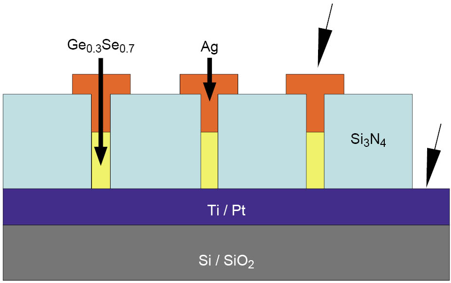
Figure 1: Schematic of the cell structure. For electrical characterization, the Pt bottom electrode was grounded.
Typical current-voltage (I-V) characteristics for a Ag-Ge-Se cell are shown in Figure 2. Initially, the film was in the OFF state. At ∼400 mV the cell switched on and reached the current compliance of 10 µA. The memory cell switched back to the OFF state at ∼−70 mV. Four point measurements revealed that as soon as the current compliance was reached, the voltage applied to the cell did not immediately drop to a constant value, but gradually decreased. This corresponds to a decrease in resistance because of the formation of a stronger conductive connection with time. We found that the write currents can be reduced significantly by introducing a GeO2 layer within the Ge0.3Se0.7 film. We assume that the GeO2 layer is a barrier for the diffusion of excess Ag into the chalcogenide layer [5]. With the leakage current in the OFF state reduced to ∼0.15 pA/µm2, resistive switching with a current compliance as low as 1 nA was possible showing cell operation with an extremely low power consumption. The write current determines the resistance of the conducting path through the solid electrolyte because its formation is dependent on the degree of oxidation and reduction. With a write current range of over more than 5 orders of magnitude, the low resistance state was variable over the same range (kΩ to several hundred MΩ) as shown in Figure 3. This increases the opportunity for multi-bit data storage in each memory cell. The low resistance state did not show a cell size dependence. Figure 4 shows the ratio of the ON resistance measured on a cell with a diameter of 2.5 µm and the ON resistance of a cell with a diameter of 50 µm as a function of the write current. The ratio does not exceed a value of 4 even though the cell cross sectional area changes by a factor of 400. This indicates that for all cell sizes only one conductive connection was established between the electrodes. The conductive path grows from the inert electrode towards the oxidizable electrode. As soon as the first ions are reduced, the electric field is highest on the tip of the growing metallic path. Therefore, this is the most probable site for further electrodeposition and only one conductive connection grows through the solid electrolyte. This is a very promising result for future downscaling, as these memory cells do not depend on material-inherent defects which might not be addressable in case of very small cells.
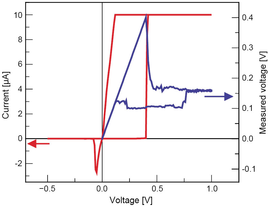
Figure 2: Current-voltage characteristics of a Ag-Ge-Se cell with a diameter of 10 µm. While the current was limited to 10 µA, the voltage gradually decreased showing that the conductive path was further strengthened after the current compliance was reached.
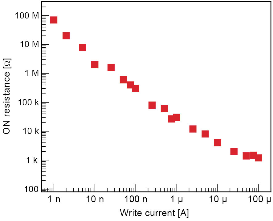
Figure 3: The ON resistance is shown versus the write current. By varying the write current, the ON resistance can be varied over five orders of magnitude.
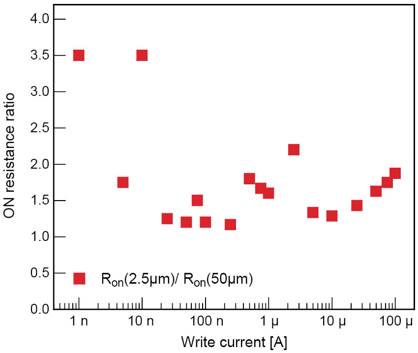
Figure 4: The ON resistance ratio of cells with a via diameter of 2.5 µm and 50 µm is shown versus the write current. Although the cross sectional area of the cells varies by a factor of 400, the ON resistance does not vary by a factor of more than 4, suggesting that only one conductive path forms between the electrodes.
Devices based on Cu-SiO2 showed very similar switching characteristics as cells based on Ag-Ge-Se [4]. The write currents could be varied over the same range as for the Ag-Ge-Se cells and even at 1 nA resistive switching could be observed. Figure 5 shows the I-V plot for a Ag-Ge-Se and a Cu-SiO2 cell which were both written with a current of 1 nA. The switching voltages and erase current level were very similar, which suggests that the switching mechanism in the Cu-SiO2 cells is based on the formation and rupture of a Cu connection between top and bottom electrode. These cells are promising candidates for future integration as they are based on materials already available in the current CMOS line.
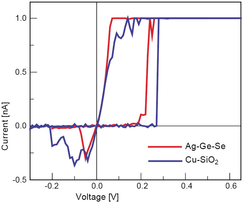
Figure 5: Typical current-voltage characteristic of a resistively switching Ag/Ag-Ge-Se/Pt and Cu/Cu-SiO2/Pt cell with a via diameter of 10 µm (Ag-Ge-Se) and a top electrode diameter of 150 µm (Cu-SiO2). The Pt electrode was grounded. The write current was limited to 1 nA.
- [1] M. N. Kozicki, C. Ratnakumar, M. Mitkova, Proceedings of the 7th Non-Volatile Memory Technology Symposium (NVMTS), 111–117 (2006)
- [2] K. Terabe, T. Hasegawa, T. Nakayama, M. Aono, Nature 433 (2005)
- [3] C. Schindler, S. P. Puthen Thermadam, R. Waser, M. N. Kozicki, IEEE Transactions on Electron Devices 54, 2762–2768 (2007)
- [4] C. Schindler, M. Meier, M. N. Kozicki, R. Waser, Proceedings of the 8th Non Volatile Memory Technology Symposium, (2007) in press
- [5] C. Schindler, X. Guo, A. Besmehn, R. Waser, Z. Phys. Chem. 221, 1–10 (2007)
C. Schindler, M. Weides, M. Meier, R. Waser
Electrochemical Fabrication and Characterization of Nanocontacts for Single Organic Molecules and Nanoclusters
Cu nanocontacts and molecular-sized nanogaps were prepared and characterized at electrified solid/liquid interfaces employing lithographic and electrochemical techniques. A dedicated four-electrode potentiostat was developed for controlling the electrochemical fabrication process and for monitoring the electrical characteristics. The formation and breaking of Cu nanocontacts exhibit conductance quantization. The statistical analysis of conductance histograms revealed a preferential stability of nanocontacts with 1 Go, 2 Go and 3 Go. The growth of molecular-sized gaps shows quantized tunneling current.
As the miniaturization of electronic components approaches the nanometer scale new concepts to tailor structure, functionality and fabrication strategies are essential. The bottom up assembly of well-defined nanoscale building blocks, such as tailored molecules, nanocrystals, quantum dots, and nanowires represents an important topic in both fundamental and technology-relevant research [1]. One of the major challenges in producing nanoscale electronic devices is the reliable fabrication of nanometer-sized metal electrodes that enable electrical contact to individual chemical nanostructures. Different approaches have been developed to fabricate electrode pairs with molecular scale gaps and metal nanocontacts. Strategies based on electrochemical concepts involve local probe techniques or supported electrodes on solid substrates [2]. A unique advantage of these electrochemical fabrication methods is the reversibility, i.e. nanostructures can be tuned by electrodeposition and dissolution until the most desirable structure is created. Simultaneously, the electron transport properties are monitored.
Here we report on the development of a custom-designed low current bipotentiostat for the electrochemical fabrication and characterization of nanocontacts and molecular-sized gaps. As an example of applications, the formation and dissolution of copper nanocontacts will be described.
Substrate: Template chips were fabricated employing electron beam and optical lithography in combination with standard lift off techniques. The substrate was covered with a thermally grown silicon oxide layer of 400 nm thickness. The electrodes and leads were prepared by sequential vaporation of Ti (2 nm), Pt (5 nm) and Au (50 nm) ontop, deposition rate < 0.05 nm s−1. The initial separation of the nanoelectrodes varied between 20 nm and 60 nm. All nanoelectrodes were connected via gold leads to macroscopic contact pads. The entire chip was protected with a coating of hard-baked PMMA, except the access windows of approximately 700 nm × 700 nm around each pair of nanoelectrodes and the contacts (Figure 1, [3, 4]).
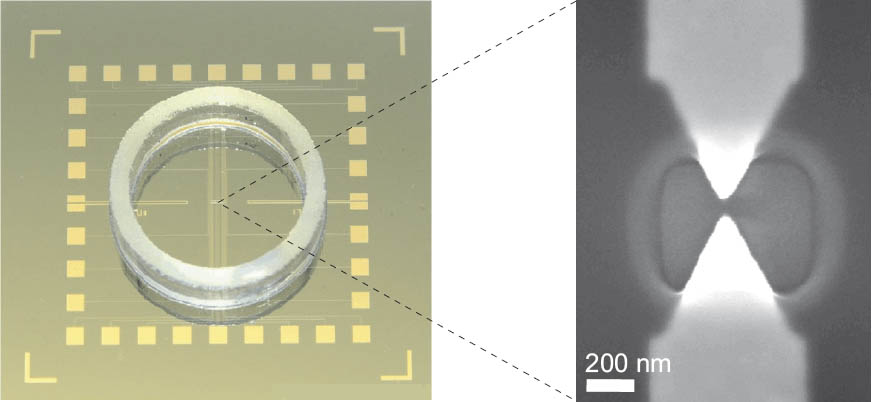
Figure 1: Photograph of the chip assembly with glass ring and Scanning Electron Micrograph of a pair of gold electrodes with access window; scale bar 200 nm.
Bipotentiostat: A low current four-electrode bipotentiostat and custom-made software were developed to control the electrochemical fabrication process and to monitor the electrical characteristics of the created nanostructures [4, 5]. The current input stages of the bipotentiostat consist of two temperature-stabilized logarithmic current-to-voltage converters with a maximum resolution of approximately 5 fA (with 0.8 s integration time) and a time constant of ∼2 ms in the low pA range, accuracy of the current < 2 % in 10 pA ≤ i ≤ 2 mA. All signals are digitized by a 16 bit A/D converter while the controlling signals are supplied by 16 bit D/A converters. All timing and data collection tasks are performed by an 8 bit microcontroller that connects to a PC via a galvanically isolated USB interface. A separate analog sweep generator operates in the range between 1 mV s−1 and 10 V s−1.
Copper nanocontacts, quantum tunneling and quantum conductance: The formation of Cu nanocontacts was achieved by depositing Cu on one electrode (WE1) only of each pair of pre-fabricated nanoelectrodes (WE1, WE2). The potential of the other electrode WE2 was typically held at values slightly negative of the (1 × 1) Cu UPD phase, which ensures a negligible low Cu deposition rate. Four phases of electrodeposition corresponding to different ranges of the electrode separation can be identified from the entire evolution of the monitor current (Figure 2):
In the first phase I, the dc current at WE1 is rather constant and typically < 100 pA being determined by the diffusion-controlled deposition of Cu onto the electrolyte exposed surface of WE1 (Faraday current). The current at WE2 is two to three orders of magnitude smaller.
The second phase II is characterized by an exponential, but step-wise increase of the current up to several hundred nA (inset A in Figure 2), which is attributed to direct tunneling between the two working electrodes. The proof for direct tunneling was obtained by ramping the bias voltage Ebias = EWE2 − EWE1. The potential of WE1 was kept constant at EWE1 = −0.163 V, e.g. in the Cu OPD region, while the potential of WE2 was scanned with 20 Vs−1. The inset B in Figure 2 illustrates a current vs. bias voltage plot of an advanced stage of the deposition on WE1. The nonlinear current increases several orders of magnitude from nA to the µA range. The quantized tunneling current (inset A in Figure 2) is attributed to the discrete nature of Cu atoms and molecular (water) respective ionic adsorbates in the junction. The width of the gap was estimated based on the measured current – time characteristics assuming a tunneling coefficient κeff ∼ 10 nm−1 and zero gap width at quantum point contact. We could stabilize molecular sized gaps typically for t ≤ 1 s without applying an external feedback signal [4].
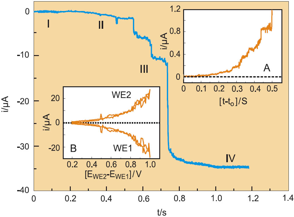
Figure 2: Current-time traces of formation of a Cu quantum wire fabricated on a pair of gold template electrodes in 0.1 MH2SO4 + 1 mM CuSO4. The four phases of electrodeposition are labeled I to IV. The Cu OPD deposition was initialized by stepping the potential of EWE1 to −0.250 V (20 ms). The subsequent growth was monitored for EWE1 = −0.163 V and EWE2 = −0.050 V. The insets A illustrate the exponential, but stepwise increase of the tunneling current at Ebias = 0.113 V, inset B shows the bias dependence of the tunneling current, both recorded in region III.
The third phase labeled III is initialized by a sudden step in the current-time function followed by a sequence of additional steps which are separated by plateaus of variable length. The first current step marks the formation of an atomically thin Cu contact. The height of the first discontinuous step varies between currents corresponding to 0.1 Go up to values close to 1 Go, depending on the atomic configuration of the respective tunneling junction. Further deposition results in an increase in the diameter of the “nanowire” that bridges the two electrodes during which the conductance current increases in a stepwise sequence until a continuous response in phase IV is reached. The growing wire exhibits finally macroscopic ohmic behavior. The limiting current in region IV is used to estimate the series resistance of the connecting leads, which contact the nanowires formed in phase III.
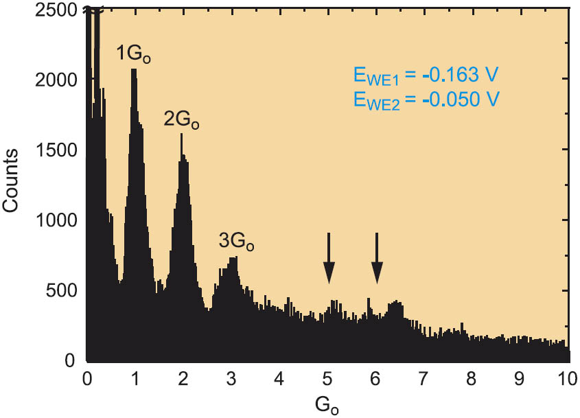
Figure 3: Conductance histogram for the repeated formation of Cu nanowires constructed from 100 individual traces. For other conditions c.f. Figure 2.
The current and the corresponding recalculated conductance of several hundreds of deposition and dissolution traces were analyzed quantitatively by constructing conductance histograms. A typical result is displayed in Figure 3. The first three peaks are well resolved at 1 Go, 2 Go and 3 Go. Less pronounced peaks were found at higher integer numbers. The statistical analysis did not provide evidence for fractional conductance peaks below 5 Go for bias voltages smaller than 0.150 V. Because each abrupt conductance step corresponds to a rearrangement in the atomic configurations of the fabricated nanoelectrodes, we conclude that 1 Go, 2 Go and 3 Go represent particular stable atomic configurations of the Cu wires fabricated under our experimental conditions.
Sustainable Cu nanocontacts and nanogaps were prepared by potentiostatic electrodeposition of Cu onto Au wires supported on an insulating solid substrate. Despite the still existing limitations in the long-term stability of nanocontacts and molecular-sized gaps, we have established in this research the principles for fabricating stable nanogaps in an electrochemical environment. The strategy developed provides the basis for further functionalization of the nanoelectrode assemblies with nanoscale objects, such as tailored molecules, clusters or nanotubes.
- [1] Encyclopedia of Nanoscience and Nanotechnolgy, H. S. Nalwa ed., American Scientific Publishers, Valencia, (2004)
- [2] C. Z. Li, H. X. He, N. J. Tao, Appl. Phys. Lett. 77, 3995 (2000)
- [3] S. Kronholz, S. Karthäuser, A. v. der Hart, T. Wandlowski, R. Waser. Microelectronics J. 37, 591 (2006)
- [4] G. Meszaros, S. Kronholz, S. Karthäuser, D. Mayer, T. Wandlowski, Appl. Phys. B, in press (2006)
- [5] G. Meszaros, C. Li, I. Pobelov, Th. Wandlowski, Rev. Sci. Instr., in preparation
G. Meszaros1, S. Kronholz, S. Karthäuser, D. Mayer, Th. Wandlowski
1Chemical Research Center, Hungarian Academy of Sciences, Budapest