complex oxide interfaces - valency changes and metal-insulator transitions
Transition metal oxides (TMO), in particular perovskite-structured crystals, exhibit a broad variety of interesting phenomena such as charge- and spin-density waves, Jahn-Teller distortions, colossal magnetoresistance, unusual metal-insulator transitions, and superconductivity. These phenomena arise from the d-orbitals of TM cations which are both very tightly localized and highly directional, leading to narrow electronic bands and strong electron-electron interaction. In recent years, more unexpected effects have been discovered in layered structures, hetero-interfaces, and artifical superlattices which comprise 2-D electron gases, charge ordering, electronic and atomic reconstructions, correlated electron effects, as well as field effects. We aim at applying our expertise in the area of lattice disorder thermodynamics of transition metal oxides to oxide heterostructures and artifical superlattices in order to explore the physics of the 2-D effects and related phenomenon. In addition, we are interested in the interplay between ferroelectric polarization and hetero-interface charges. Despite the fact that this research is curiosity-driven and fundamental, we are searching for paths on which the results of these studies can be utilized for novel nanoelectronic devices.
Effect of Charge Compensation Mechanisms on the Conductivity at LaAlO3/SrTiO3 Interfaces
The equilibrium high temperature conductance (HTEC) of LaAlO3/SrTiO3 (LAO/STO)-hetero-interfaces was investigated as a function of ambient oxygen partial pressure (pO2). Metallic conducting interfaces were obtained for LAO grown on STO single crystals as well as on STO-buffered LSAT substrates. For both structures, the high temperature sheet carrier density nS of the LAO/STO-interface saturates at a value of about 1×1014 cm-2 for reducing conditions, which indicates the presence of interfacial donor states. A significant decrease of nS is observed at high oxygen partial pressures. According to the defect chemistry model of donor-doped STO, this behavior for oxidizing conditions can be attributed to the formation of cation vacancies as charge compensating defects.
The role of defects is a focus of the ongoing discussion about the electronic properties of the conducting interface between the two insulators LaAlO3 (LAO) and SrTiO3 (STO). Besides the model of charge transfer due to the polar nature of LAO, it is generally accepted that defects in the vicinity of the LAO/STO interface can have a large impact on the electronic properties. At the extreme, the interdiffusion of La-ions on Sr-sites (LaSr•), and the creation of oxygen vacancies (VO••) within the STO lattice, have even been considered as sole origin of the interface conduction.
In this study, the LAO/STO-interface is discussed from a defect chemical point of view [1]. Besides the above described defects, also cation vacancies in the STO lattice, i.e. Sr-vacancies (VSr′′) and Ti-vacancies (VTi′′′′), were considered in order to draw a complete picture of the LAO/STO-interface (see Figure 1). The conducting LAO/STO-interfaces are fabricated by pulsed laser deposition (PLD) of LAO on TiO2-terminated STO single crystal substrates, and by the heteroepitaxial growth of LAO and STO on LSAT ((La,Sr)(Al,Ta)O3) single crystal substrates. Both types of heterostructures show metallic conductance behaviour at low temperatures as revealed by Hall measurements. In contrast to the standard LAO/STO-heterostructure, the electron mobility at the LAO/STO-interface on LSAT exhibits only a weak temperature dependence [2]. This indicates a more defective interface region originating from the STO growth process [3].
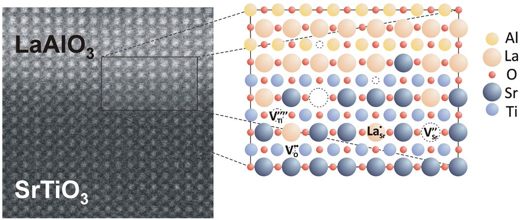
Figure 1: HAADF-image of the LAO/STO-interface (from Ref. [4]) and a schematic illustration of possible defects in the STO lattice close to the interface: Oxygen vacancies (VO••); interdiffused La-dopants (LaSr•); Sr-vacancies (VSr′′); Ti-vacancies (VTi′′′′).
The particular defect structure of the LAO/STO-interface was investigated by means of high temperature conductance measurements in equilibrium with the surrounding atmosphere (HTEC). In the studied temperature range (950 K–1100 K), the decisive defect reactions at the LAO/STO-interface are activated, and hence, strive for a well-defined thermodynamic equilibrium state, which is related to the ambient oxygen pressure (pO2). The resulting conductance characteristics contain information about the chemical reactions, which take place at the LAO/STO-interface, and the corresponding defect concentrations. Using this method, we could exclude that mobile oxygen vacancies are the sole origin of the electronic charge carriers at the interface [4]. In fact, the temperature- and oxygen partial pressure independent plateau region, which is found for reducing atmospheres, indicates the presence of immobile donor states (D•) close to the interface. In the pO2-independent plateau region, the sheet electron density nS approaches a value of 1×1014 cm-2 for both samples (LAO/STO and LAO/STO/LSAT). This value is consistent with the carrier densities obtained from low temperature Hall measurements [2] as well as from spectroscopic investigations [5].
The HTEC measurements on LAO/STO systems grown on LSAT substrates additionally revealed a very interesting feature at oxidizing conditions. The observation of this effect was possible due to the low intrinsic conductance of the LSAT single crystal, while, for the standard LAO/STO-system, the interface behaviour under oxidizing conditions is mainly hidden by the large intrinsic conductance contribution of the SrTiO3 single crystal [4].
Starting from the plateau region at low oxygen partial pressure (see Figure 2), the interfacial electron density starts to decrease for increasing pO2. This decrease becomes proportional to pO2−1/4 for higher oxidizing conditions. In this region, nS is no longer temperature independent. In contrast, nS is thermally activated exhibiting an activation energy EA of approximately 1 eV. As will be discussed below, this change of behaviour can be seen as an indication for the formation of additional defects in the vicinity of the LAO/STO-interface.
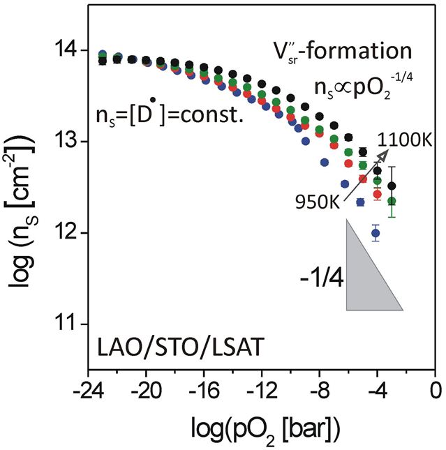
Figure 2: pO2-dependence of the sheet carrier density, nS, of the LAO/STO interface on LSAT obtained from HTEC measurements (from Ref. [1]); A pO2- and temperature independent region is found for reducing conditions indicating the presence of interfacial donor states (D•). For oxidizing atmosphere, nS decreases proportional to pO2−1/4 which can be attributed to the formation of acceptor-like Sr-vacancies.
The measured HTEC characteristics of the LAO/STO interfaces resemble in good agreement the HTEC behavior of donor-doped STO [6]. Therefore, the corresponding defect chemistry model was transferred to the LAO/STO heterostructures. In the pO2-independent region, each donor is compensated by a free electron which contributes to the interface conduction (full electronic compensation). This can be expressed by the charge neutrality condition n = [D•], whereas the concentration of extrinsic donors [D•] is considered as a pO2-independent parameter.
In order to maintain charge neutrality, the observed decrease of n below the donor level [D•] requires the formation of additional compensating defects which carry a negative net charge. This yields to the conclusion that cation vacancies, either Sr-vacancies (VSr′′) or Ti-vacancies (VTi′′′′), have to be considered as acceptor-type electron traps in the vicinity of the LAO/STO-interface [1]. Considering this scenario, the defect chemistry model of STO predicts a decrease of the electron density proportional to pO2-1/4 (in the limiting case of a full ionic compensation of the extrinsic donors). Hence, the observation of this characteristic behaviour can be regarded as an indication of the formation of cation vacancies in the vicinity of the LAO/STO-interface in oxidizing atmosphere.
The in-situ study of the HTEC of LAO/STO-heterostructures emphasizes the importance of crystal disorder for the electronic properties of the LAO/STO-interface. The observed pO2- and temperature-independence of the sheet electron density for reducing conditions supports the idea of a donor-type conduction mechanism at the LAO/STO-interface such as provided by cation-intermixing. Furthermore, the decrease of nS in oxidizing conditions indicates a complex charge compensation mechanism in the vicinity of the interface, which involves the formation of cation vacancies at high oxygen partial pressures. This implies that oxygen annealing after the growth of LAO/STO-heterostructures – which is commonly thought to merely remove oxygen vacancies from the STO substrate – can also result in an increased cation vacancy concentration at the interface. These additional defects can reduce the electron density and, moreover, can act as scatter centers at low temperatures.
As pivotal result of this study, it has been shown that in the vicinity of the LAO/STO-interface exchange reactions in the cation sublattice, i.e., formation and annihilation of strontium vacancies take place at typical growth temperatures and have to be considered in the discussion of the LAO/STO interface.
This work was performed during a bilateral collaboration of the PGI-7 and the MESA+ Institute of the University of Twente, Enschede.
- [1] F. Gunkel P. Brinks, S. Hoffmann-Eifert, R. Dittmann, M. Huijben, J. E. Kleibeuker, G. Koster, G. Rijnders, and R. Waser., Appl. Phys. Lett. 100, 052103 (2012).
- [2] P. Brinks, W. Siemons, J. E. Kleibeuker, G. Koster, G. Rijnders, M. Huijben, Appl. Phys. Lett. 98, 242904 (2011).
- [3] D. J. Keeble, S. Wicklein, R. Dittmann, L. Ravelli, R. A. Mackie, and W. Egger, Phys. Rev. Lett. 105, 226102 (2010).
- [4] D. J. Keeble, S. Wicklein, R. Dittmann, L. Ravelli, R. A. Mackie, and W. Egger, Phys. Rev. Lett. 105, 226102 (2010).
- [5] G. Berner, S. Glawion, J. Walde, F. Pfaff, H. Hollmark, L. C. Duda, S. Paetel, C. Richter, J. Mannhart, M. Sing, and R. Claessen, Phys. Rev. B 82, 241405 (2010).
- [6] R. Moos and K. H. Haerdtl, J. Am. Ceram. Soc. 80, 2549 (1997).
F. Gunkel, P. Brinks1, S. Hoffmann-Eifert, R. Dittmann, M. Huijben1, J. E. Kleibeuker1, G. Koster1, G. Rijnders1, and R. Waser
1 MESA+ Institute for Nanotechnology, University of Twente, The Netherlands
SrZrO3 nanopatterning using self-organized SrRuO3 as template
TASK
Several characteristics such as high dielectric constant and high breakdown strength make SZO particularly suitable for high voltage and high reliability capacitive applications. In addition SZO thin films with transition metal doping are possible candidates for use in nonvolatile random access memories. To come up with demanded memory densities for the future memory cell sizes in the nanometer range are required. An advantageous fabrication route for such nanostructures is provided by self-organized deposition techniques, which have to be adopted to perovskite oxides.
APPROACH
Self-organized deposition techniques, which take advantage of periodic arrangements of kinks and steps as well as stress-induced surface modulations have been employed to fabricate nanostructures of SZO. The ability of the heteroepitaxial SZO/SRO system to self-organize into arrays of ordered nanostructures driven by a high degree of lattice mismatch was investigated. The crystal structure and the morphology of thin films of SZO prepared by pulsed laser deposition (PLD) on SRO/STO substrates were studied by XRD analysis, RBS, AFM and HRTEM methods.
RESULTS
The SRO growth mode has been conveniently tailored using a phototreated STO surface such that the step-flow mode is replaced (i.e., inhibited) by a laterally confined 3D growth habit. This growth mode takes advantage of the periodic features on the departing surface, which operates as confinement boundaries, to give rise to self-organized (rippled) films. The so-deposited samples serve as nanoscale template for the growth of successive patterned oxide layers, for instance, SZO was deposited forming a dielectric nanowire array. SZO can be epitaxially and stoichiometric grown on the SRO layer despite the lattice mismatch of about –4.5% between SZO and SRO. The first growth stages of SZO have been identified by AFM with conductive tip an basis of the difference between the electrical conductivities of SZO and SRO. Dielectric nanowires of SZO grown on the self-organized rippled SRO and separated by deep and narrow boundaries that extend down to the conductive SRO layer can be fabricated.
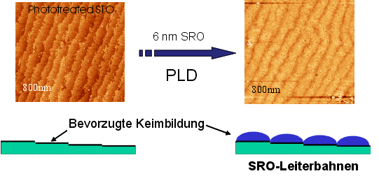
Figure 1:
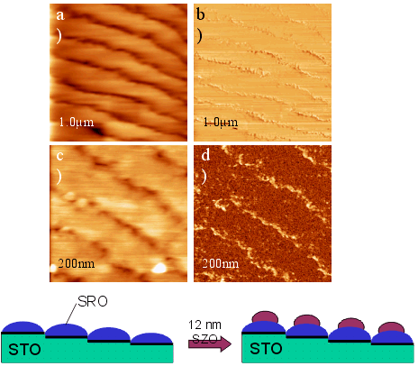
Figure 2:
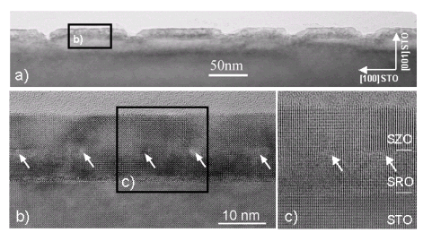
Figure 3:
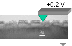
Figure 4:
E. Vasco, S. Karthäuser, R. Dittmann
Segregations and Solid State Reactions in the Near-Surface Region in Perovskite Materials of ABO3 Type at Elevated Temperatures
TASK
Perovskite-type oxides ABO3 (eg. A=Sr,Ba; B=Ti,Zr) are typically regarded as highly stable compounds. However, we found strong indications that this is not valid for the near-surface region. The chemical segregation and phase sepa-ration processes have been studied in this project.
APPROACH
The complicated nature of the solid state reactions occurring in the near-surface region have been analyzed with a variety of surface sensitive methods such as SIMS, STM, AFM, XPS and X-ray technique. In order to study the influence of different thermodynamical factors on the segregation phenomena, sin-gle crystals of model perovskites were prepared by high-temperature treatment under various reducing and oxidizing conditions. The parameters were adjusted with respect to the defect chemical diagrams for ternary oxides to test the standard point defect model. The potential influence of extended defects on the dynamics of the redistribution of chemical complexes in the surface layer were studied by tracer experiments.
RESULTS
The combination of x-ray dif-fraction analysis with surface sensitive techniques shows that a restructuring takes place in the near-surface region of stoichiometric perovskite of ABO3-type at elevated temperatures as a result of a redistribution of material and subsequent solid state reactions. This leads to a chemically inhomogeneous near-surface region in single crystals which can be charac-terised by a multilayer-type arrangement of different Ruddlesden-Popper phases (AO*(ABO3)n) and B-rich phases (BO2-x) formed by an intercala-tion and dismantling of AO-layers, respectively. The se-quence of AO-rich and B-rich phases in the near-surface region is anticorrelated for oxidizing and reducing conditions.
Under oxidizing conditions the surface of ABO3 undergoes dramatic changes due to the enrichment of AO and subsequent modifications of the topography. The ultrafast dynamics of the segregation near the surface may be related to the diffusion along extended defects. AFM images of the surface topography after thermal treatment are shown for SrTiO3 together with the schematical presentation of the redistribution reactions in the near-surface region in the figure.
Combining the available information, we postulate that the near-surface region of perov-skite materials after thermal treatment is almost always chemically heterogeneous with respect to the stoichiometric bulk. The implications for thin films are currently under study.
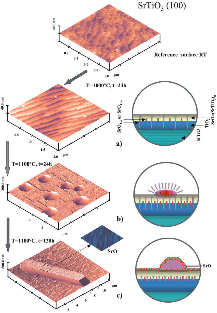
Figure 1: Schematically shown are the restructuring in the near-surface region of SrTiO3 at 1000 °C
(a) and the dynamics of the processes related with the precipitation of SrO1+δ or SrO1+δ at higher temperatures (1100 °C). Several stages in the course of heat treatment are depicted:
(b): precipitation and growth of the droplet-like features plus accompanying evaporation;
(c): recrystallization with modified surface layer preventing further loss of material.
K. Szot, W. Speier, ICG/FZ, U. Breuer, ZCH/FZ, U. Zastrow, ISI/FZJ
Nonstoichiometry of n-doped SrTiO3
TASK
SrTiO3 serves as a model material for the study of electrical properties in the perovskite system. Unlike acceptor-doped and undoped specimens, donor-doped material shows a significant nonstoichiometry in the cation sublattice. In the high temperature regime and depending on temperature and oxygen partial pressure, a formation or removal of cation vacancies takes place. While former investigations concentrated on the system's thermodynamics, the kinetics still remain uncomletely settled. Nevertheless, the most interesting effects in donor doped SrTiO3 like sensor properties or electrically active grain boundaries are based on the heterogeneous defect concentrations in the material, caused by a non-equilibrium of the sample. Due to the slow conversion in the cation sublattice, this non-equilibrium is present in most applications.
The aim of the current project is to investigate the formation mechanism of Sr vacancies VSr, and to study the kinetics of the system.
APPROACH
Kinetics
To confirm the proposed diffusion controlled mechanism of the strontium vacancy formation, the single crystal surface has to yield a SrO-rich second phase. Therefore, surface sensitive methods like optical microscopy, EDX and HRTEM were used to identify a secondary phase on the sample surface.
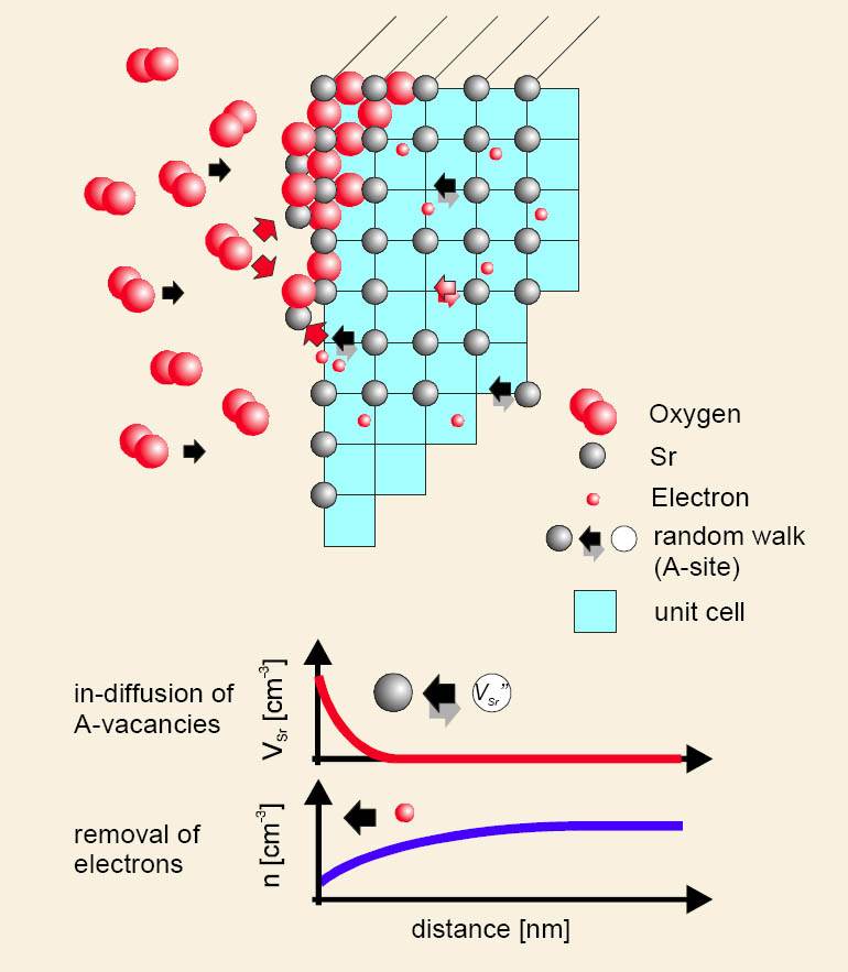
Figure 1: Basic sketch: diffusion controlled process for the incorporation of strontium vacancies
Modeling
In a second step, a finite differences program has been developed to simulate the concentration profiles for the mobile specimen strontium vacancies, electrons and oxygen vacancies. In a new approach, the surface concentrations are calculated by means of the laws of mass actions by taking into account the near-surface space charge. From the concentration pro-files, experimentally accessible variables like resistivity, weight change and 18O-tracer profiles have to be derived.
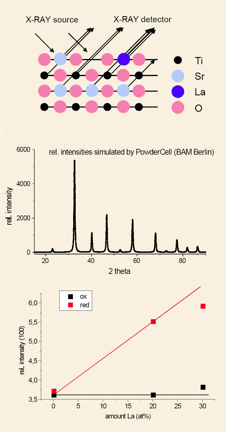
Figure 2: Identification of randomly distributed strontium vacancies by simulation(PowderCell by BAM Berlin) and experimental XRD-powder diffraction
RESULTS
Diffusion mechanism
After an oxygen anneal treatment, SrO-rich precipi-tates were found. The experi-mental observations in con-junction with thermo-gravimetry and conductivity data taken from the literature suggest that the single crystal surface acts as the source for strontium vacancies and sink for the SrO-rich second phase, respectively.
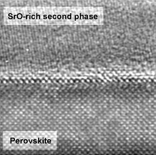
Figure 3: HRTEM image of a cross-section perovskite/SrO rich second phase
Simulation results
The diffusion profiles of all mobile specimen do not follow a simple Fick's law. Surface concentrations, calculated by the law of mass actions, significantly differ from the equilibrium values. The time dependent concentration, e.g. of the electrons, mainly influences the resistivity behavior and offers a new explanation for both redox-experiments and fast sensor responses of n-doped SrTiO3.
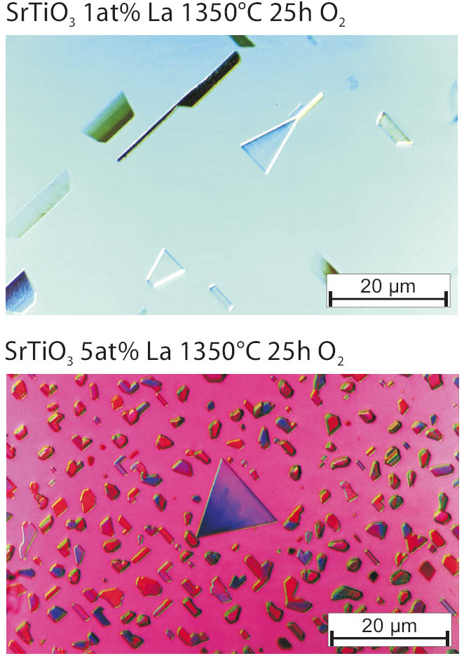
Figure 4: Optical image of single crystal surfaces showing SrO rich precipitates
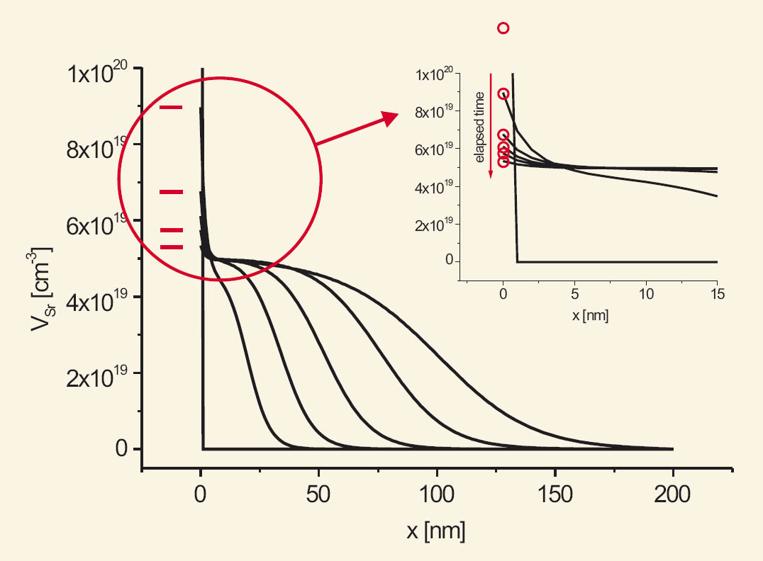
Figure 5: Simulated profile of strontium vacancies with varying surface concentration
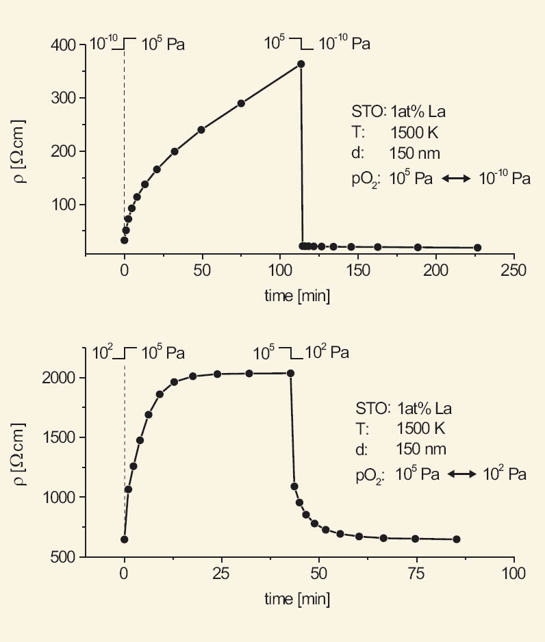
Figure 6: Simulation of an oxidation/reduction experiment for small and large changes of oxygen partial pressure, respectively
R. Meyer, R. Waser
Grain Boundary Space Charge Regions and High-Field Effects in Acceptor-Doped SrTiO3
TASK
Doped (e. g. net acceptor-doped) earth alkaline titanates are typically used as dielectrics for multilayer capacitors. The quality of these materials is improved by grain boundaries (GBs), as they increase the insulating resistance and life time under an external electrical field. Hence, a detailed understanding of the electron-ic, crystallographic and chem-ical nature of GBs plays a cru-cial role for further improve-ments of the material. Due to the trend towards further miniaturization, especially the decrease in the dielectric thickness between the internal electrodes, the electrical field stress under rated operation voltages increases (both, in the grains and at the grain bound-aries). Within this project, the electronic structure of acceptor-doped model materials (here: SrTiO3) is investigated by impedance analysis in the time and frequency domain.
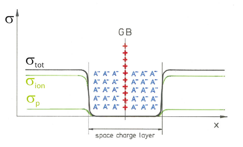
Figure 1: Sketch of the conductivity profile across a GB plane and the charges in the GB region
We discuss how the electrical properties of GBs and bulk are separated and how the influence of high electric fields on the electrical GB properties is described by suitable experimental procedures and modelling.
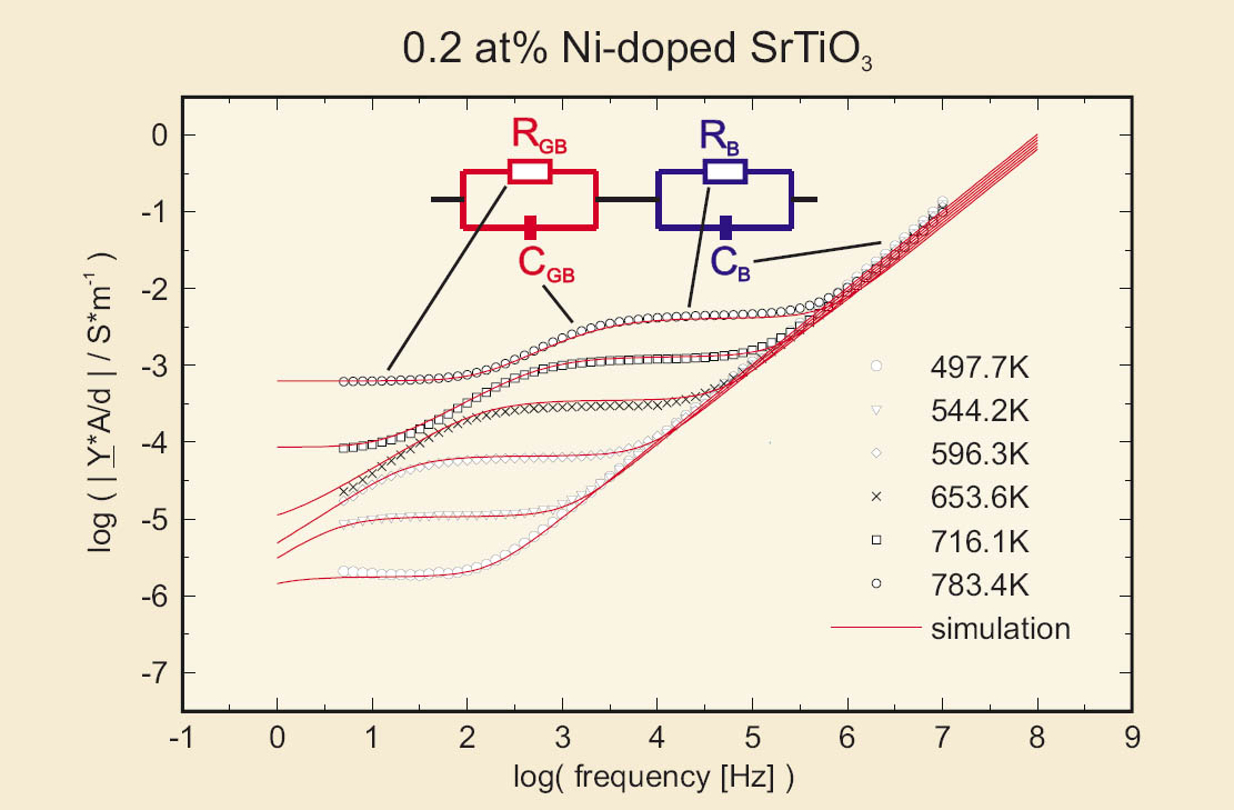
Figure 2: Impedance spectra (symbols) and simulation results (lines) for a 0.2 at% Ni-doped SrTiO3 model ceramic
APPROACH
In general, ceramics are built from grains with different shapes and grain sizes. In a simplifying brick-wall model, the ceramic is supposed to be composed of identical cubic grains separated by GBs parallel and perpendicular to the electrode interface. Based on this model, an electrical circuit, consisting of two RC branches, represents the electrical properties of the ceramic. Temperature dependent impedance spectra permit the determination of the circuit elements. In addition, the voltage-step technique allows to investigate the influence of the electrical field on the electrical properties in the long-time/low-current regime. In addition, high voltages can be applied in order to study non-linear charge transport processes. All experiments are assis-ted by simulation studies.
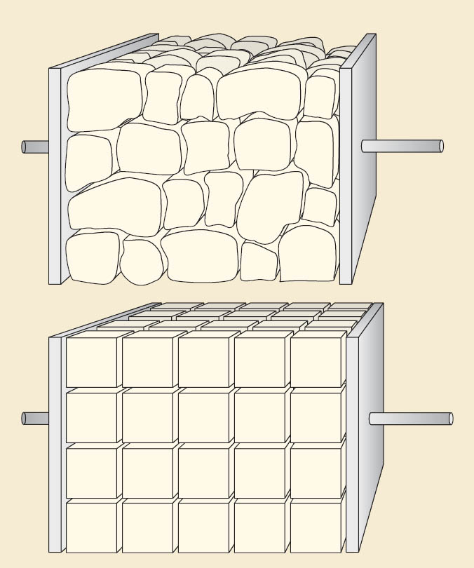
Figure 3: Real ceramic microstructure and idealized brick-wall structure.
RESULTS
The impedance data indicate the occurrence of a Maxwell-Wagner relaxation, for which the brick-wall model gives a suitable description.
The Maxwell-Wagner relaxation time τR is given by the product of bulk resistance and GB capacity. The GB capacity is due to a space charge layer region surrounding the GB. At the GB core, native donor-type, immobile charges (GB states) exist, leading to a depletion of mobile positively charged carriers (oxygen vacancies and holes) in a layer of 50–100 nm width.
The bulk conductivity σB as well as the GB conductivity σGB are thermally activated. The activation energy of σB is determined mainly by the oxygen vacancy mobility and amounts approximately 1 eV within the investigated tem-perature range between 300 and 800 K. In contrast, σGB shows two different activation energies, related to different spatial profile shapes in the GB space charge region, denoted as "V"-profile in the lower and "W"-profile in the higher temperature regime. The activation energy for the V-profile is correlated to the acceptor-state level (approx. 1 eV for our ceramics), and for the W-profile to half the band gap (about 1.6 eV). The notation stems from the shape of the overall local conductivity in a cross-section over the GB and the adjacent space charge region, as un equivocally shown by our numerical simulation.
The reason for the W-shape is a charge carrier inversion, caused by an enrichment of electrons at the GB core. This inversion gives rise to a certain part of conductivity along GBs and, for strong inversion, can by-pass the cross transport. Increasing the electrical dc field amplitude, σB remains unaffected, while σGB is increased due to the confinement of most of the field in the GB space charge region and the non-linear charge transport across the GB barrier. The field dependence can be described by an ohmic, a varistor and a saturation regime. The ohmic and high-field varistor regime can be described well by the Schottky diffusion model. A possible explanation for the saturation is the accumulation of oxygen vacancies, stabilizing the GB barrier.
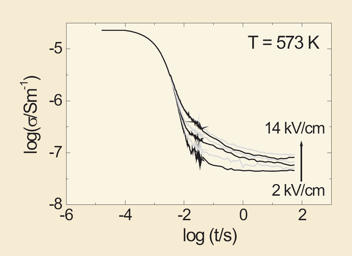
Figure 4: Voltage step results for a 0.2 at% Ni-doped SrTiO3 ceramic at fields between 2 and 14 kV/cm
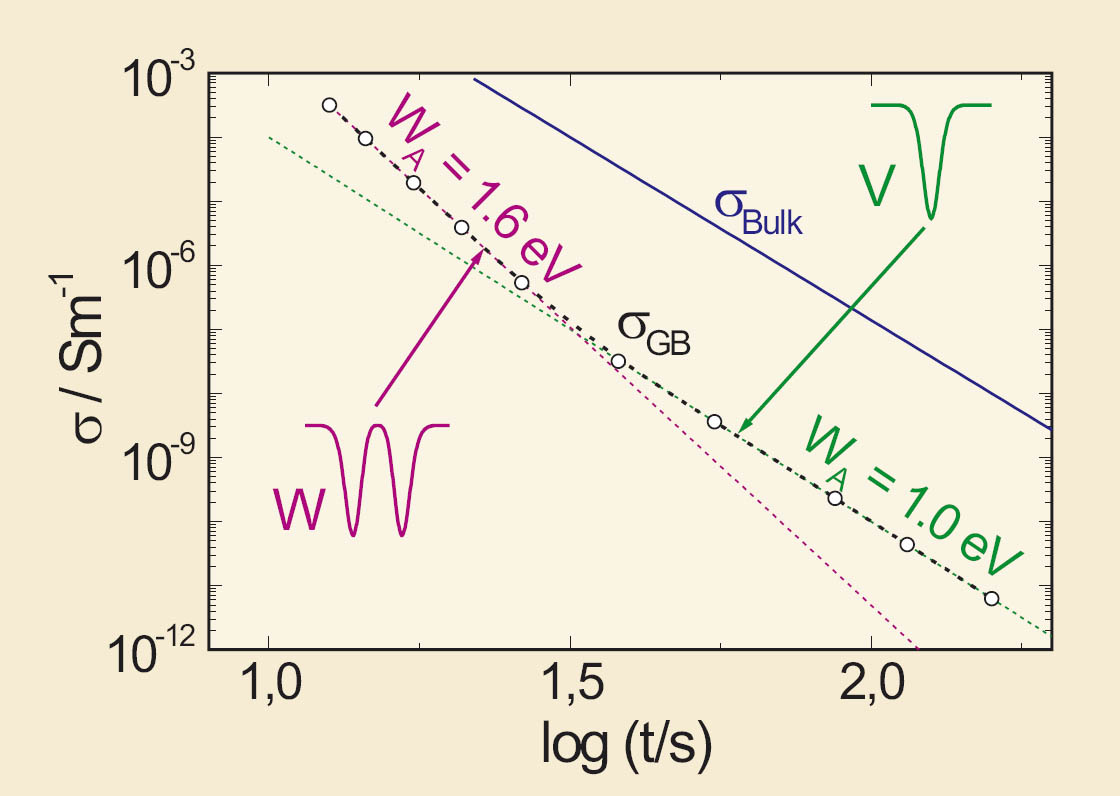
Figure 5: Arrhenius plot of σGB for a 0.2 at% Ni-doped SrTiO3 ceramic
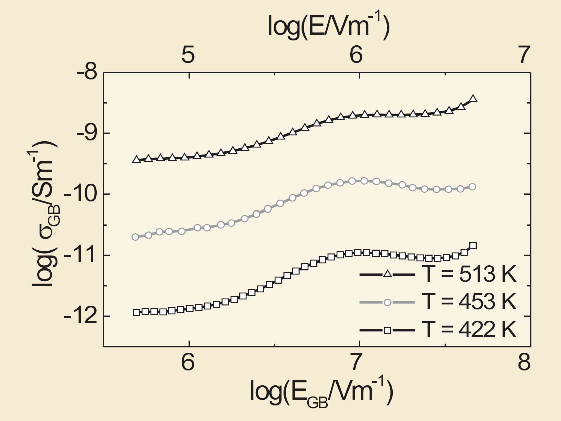
Figure 6: Field dependence of σGB at different temperatures
M. Vollmann, R. Hagenbeck, U. Weber, R. Waser
Combining Ferroelectricity, Magnetism, and Superconductivity in Tunnel Junctions
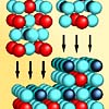
Complex oxides display a rich variety of physical phenomena including magnetism, superconductivity, and ferroelectricity. From many points of view it is an interesting approach to combine these (partly antagonistic) cooperative phenomena in tunnel junctions. On the one hand, new device functionalities are expected in such complex junctions. On the other hand, tunneling electrons are extremely sensitive to the barrier and interface excitations and, therefore, represent an ideal spectroscopic tool to extract material properties on the nanometer and even atomic scale. By combing ferroelectric or multiferroic tunnel barriers with ferromagnetic and/or superconducting electrodes, a whole “zoo” of novel tunnel junctions can be proposed.
Historically, the electron tunneling effect played a significant role for the development of quantum mechanics, because it provided proof for the particle-wave dualism [1]. Electron tunneling is described by wave functions and the Schrödinger equation. A typical tunnel junction consists of two metal layers separated by a thin insulator (tunnel barrier). Although classically forbidden, an electron can traverse a potential barrier exceeding the electron´s energy, but only for ultrathin (nanometer-thick) barriers a significant tunneling probability is expected. Famous examples are metallic tunnel junctions based on the fundamental work of I. Giaever and M. Jullière [2, 3]. Recently, researchers, armed with a variety of methods, have grown entire magnetic perovskite oxide tunnel junctions made, e.g., of (La0.67Sr0.33)CoO3 or (La0.67Ca0.33)CoO3 electrodes and SrTiO3 tunnel barriers grown on (100) single crystal SrTiO3 substrates [4]. All mentioned tunnel junctions have two features in common. First, their specific properties are associated with a cooperative phenomenon (superconductivity or magnetism), which occurs in the electrodes. Second, the barrier material in both types of junctions belongs to the group of non-polar dielectrics, although the material is very different (amorphous Al2O3 vs. single-crystalline SrTiO3).
Here we consider another, very interesting type of tunnel junction, where a ferroelectric is used as the barrier material. The concept, here termed a ferroelectric tunnel junction (FTJ), is illustrated in Figure 1 [5]. This device can be used to study the interplay of ferroelectricity and electron tunneling. It may be noted that the discovery of ferroelectricity goes back to 1920 [6], i.e., approximately to the time period when the principles of quantum mechanical electron tunneling [1] have been formulated.
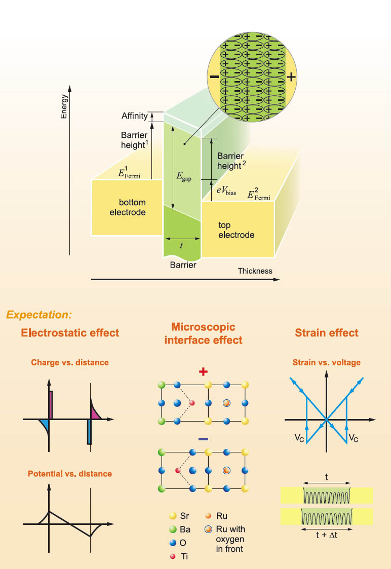
Figure 1: Schematic of a ferroelectric tunnel junction and possible effects of polarization switching on the electron transport.
Ferroelectricity is defined as a polar state of a material which can be reversed by an external electric field. The remanent polarization is typically in the range of tenths of µC/cm2. The central question is: How a ferroelectric tunnel barrier modifies the electron tunneling transport in comparison to a non-polar dielectric? Since ferroelectrics possess several specific physical properties, the current-voltage characteristics of FTJs are expected to be different from those of conventional metal-insulator-metal junctions. In particular, the electric-field-induced polarization reversal in a ferroelectric barrier may have a pronounced effect on the conductance of a FTJ and may lead to resistive switching at the coercive field of the ferroelectric material. Indeed, the polarization switching alters the sign of polarization charges existing at a given barrier/electrode interface, changes positions of ions in ferroelectric unit cells, and modifies lattice strains inside the barrier. The polarization reversal, therefore, is expected to change the tunneling transmission coefficient and so may lead to a resistive switching at the coercive voltage [7, 8].
In order to realize a FTJ, a crucial condition has to be fulfilled, i.e., ferroelectricity must exist in films which are only a few unit cells thick. Experimental evidence has been obtained by several groups. [9, 10] The modern theoretical studies, performed either using the mean-field theory [11] or employing the first-principles approach [12], also support the existence of ferroelectricity in ultrathin films. Moreover, ferroelectricity has been observed experimentally in monolayers of polyvinylidene fluoride (PVDF) [13], which is a ferroelectric polymer and so represents completely different material class. Thus, the experimental and theoretical results indicate that FTJs may be realized in practice.
In the above discussion, the electrodes in a FTJ were assumed to be in the normally conducting and paramagnetic state. Evidently, by replacing the paramagnetic electrodes in the FTJ by ferromagnets or superconductors, new types of tunnel junctions may be created (see Figure 2) [14, 15]. In these novel junctions, where the cooperative phenomena simultaneously exist in both the electrodes and the barrier, we can expect new physical effects. In particular, the electrostatic effect resulting from incomplete screening of the polarization charges at the barrier surfaces by the free charges in the electrodes [7, 8] may be very different in junctions with magnetic and/or superconducting electrodes. This “screening” effect may be pronounced in case of correlated oxide material electrodes because of their relatively low carrier density in comparison with metallic electrodes and sensitivity to external parameters. The influence of incomplete screening on the tunnel current can be considered as an electric field effect caused by the charge distribution at the ferroelectric/electrode interfaces. Moreover, an ionic screening effect existing within the first subsurface unit cells in the electrode was proposed recently [16]. Since the band structure is related to the mutual positions of atoms, a novel magnetoelectric interface effect has been predicted in case of magnetic electrodes [15].
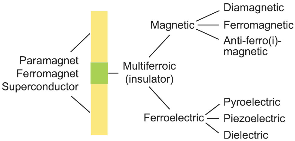
Figure 2: The “zoo” of novel tunnel junctions.
By looking even further into the future, we can predict the following scenarios. Many different material combinations in the electrode-insulator-electrode junctions are possible. Multiferroic [17] tunnel barriers, which exhibit simultaneous magnetic and ferroelectric properties, are challenging. Screening effects, strain and electric-field dependences of their properties could lead to interesting new phenomena. Multiferroic tunnel barriers in combination with superconducting electrodes are another exciting topic [17]. Probably the Josephson current as well as quasi-particle current will be influenced by the polar and magnetic nature of the barrier. Moreover, the multilayer junctions would offer even a higher degree of freedom.
So far, there is no firm experimental evidence of even a single functioning FTJ or multiferroic junction. Many obstacles have to be overcome to realize and to prove the existence of these novel types of junctions. In addition, much better understanding of the polarization switching in nanometer-thick ferroelectric films is essential. On the other hand, tremendous achievements in the field of complex oxide epitaxy, the research on ultrathin ferroelectric polymers as well as the advent of advanced analytical methods (e.g., piezoresponse force microscopy) during the last years give hope that the realization of FTJs and multiferroic junctions might soon be possible. An important point is that parasitic effects, such as local conduction and inelastic electron transport via localized states, have to be eliminated. Conversely, if FTJs or multiferroic junctions really exist, we can use the tunneling electrons as an ultra-sensitive analytical tool to study ferroelectricity and magnetism on an Angstrom and nanometer scale. In other words, the powerful tool of electron tunneling spectroscopy can be directly transferred to several kinds of novel tunnel junctions with new and fascinating properties.
- [1] J. Frenkel, Phys. Rev. 36, 1604 (1930)
- [2] I. Giaver, Phys. Rev. Lett. 5, 147 (1960)
- [3] M. Jullière, Phys. Lett. A 54, 225 (1960)
- [4] Y. Lu, et al., Phys. Rev. B 54, 8357 (1996)
- [5] E. V. Tsymbal and H. Kohlstedt, Science 313, 181 (2006) and reference therein
- [6] J. Valasek, Phys. Rev. 17, 475 (1921)
- [7] H. Kohlstedt et al., Phys. Rev. B 72, 125341 (2005)
- [8] M. Y. Zhuravlev et al., Phys. Pev. Lett. 94, 246802 (2005)
- [9] T. Tybell, C.-H. Ahn, and J. M. Triscone, Appl. Phys. Lett. 75, 856 (1999)
- [10] D. D. Fong, et al, Phys. Rev B 72, 020406 (2005
- [11] A. G. Zembilgotov, N. A. Pertsev, H. Kohlstedt, and R. Waser, J. Appl. Phys. 91, 2247 (2002)
- [12] J. Junquera and Ph. Ghosez, Nature 422, 506 (2003)
- [13] A. V. Bune, et al., Nature 391, 874 (1998)
- [14] M. Indlekofer and H. Kohlstedt, Europhys. Lett. 72, 282 (2005)
- [15] C. G. Duan et al., Phys. Rev. Lett. 97, 047201 (2006)
- [16] G. Gerra et al., Phys. Rev. Lett. 96, 107603 (2006)
- [17] M. Gajek et. al., cond-mat/060644 and references therein
H. Kohlstedt1, N. A. Pertsev1,2, A. Petraru1, U. Poppe1, R. Waser1, E. Y. Tsymbal3
1CNI – Center of Nanoelectronic Systems for Information Technology (IFF-6)
2A.F. Ioffe Physico-Technical Institute, Russian Academy of Sciences, 194021, St. Petersburg, Russia
3Department of Physics and Astronomy, Nebraska Center for Materials and Nanoscience, University of Nebraska, Lincoln, NE 68588 USA