polar oxides - exploiting ferroelectric and piezoelectric effects
Ferroelectricity is a cooperative phenomenon in the crystal lattice of polar materials, e. g. specific perovskite structured oxides ABO3 where, for example, A = Ba, Pb, etc. and B = Ti, Zr, etc. Ferrolectric.polarization arises from a tiny, spontaneous displacement of the cation and the oxygen ion sub lattices, cooperative for all lattice cells within a ferroelectric domain. Our research aims at finding and understanding the scaling limits at which the ferroelectric effect fades due to a shortage of interacting unit cells. In addition, we are studying the effect of the atomic structure and composition of the electrode interface on the local polarization, the formation of the depolarizing field, and multiferroic interactions. Furthermore, we are interested in the dynamics of the ferroelectric switching, i. e. in the details of the domain wall motion and the kinetics of the polarization reversal. As a basic concept of our projects, our goal is to use the progress in the physics of ferroelectrics to understand and improve the performance of devices such as ferroelectric random access memories or piezoelectric actuators.
Unit-Cell Scale Mapping of Ferroelectricity in Epitaxial Ferroelectric Films
By means of high-resolution transmission electron microscopy we map, on the unit-cell scale, the displacements of cations away from the centrosymmetry positions in an ultra-thin epitaxial PbZr0.2Ti0.8O3 film on a SrRuO3 electrode layer deposited on a SrTiO3 substrate. Based on the off-centre displacements of the cations local polarization in the film is estimated. A systematic reduction of the atomic displacements is measured at the interfaces. This suggests that interface-induced suppression of the ferroelectric polarization plays a critical role in the size effect of nanoscale ferroelectrics.
Epitaxial ultra-thin films of ferroelectric oxides have attracted considerable attention with respect to potential applications in nanoelectronic high-density memory devices. The magnitude and stability of the switchable ferroelectric polarization are the central figures of merit for such devices. How the polarization scales with reduced thickness, particularly when the film thickness becomes smaller than typically 10 nm, is now an intensely debated topic. This so-called “size effect” represents one of the most intriguing phenomena in the area of thin-film ferroelectrics.
The switchable polarization, ΔP, is ideally twice the remnant polarization or spontaneous polarization, PS, which arises as a result of the separation of the charge centre of cations from that of anions. Therefore, the local polarization of the film can in principle be investigated by measuring the atomic displacements. In the present work, we map the atomic displacements of the cations by high-resolution transmission electron microscopy (HRTEM) and thus investigate at the unit-cell scale the polarization in an epitaxial ultra-thin, about 7 nm thick, film of PbZr0.2Ti0.8O3 (PZT) on an SrRuO3 (SRO) electrode deposited on a SrTiO3 substrate using a 400 kV electron microscope.
Figure 1 shows schematically the tetragonal unit cell of ferroelectric PZT (a) and the unit cell of the underlying SRO electrode (b) in a projection along the crystallographic b-axis. We point out that in reality even the lattice of the SRO electrode shows tetragonal symmetry due to the in-plane constraint imposed by the SrTiO3 (STO) substrate. In PZT the position of the Zr/Ti atoms (red) as well as that of the O atoms (blue) is displaced along the c-axis direction by a distance δZr/Ti and δO with respect to the positions of centrosymmetry.
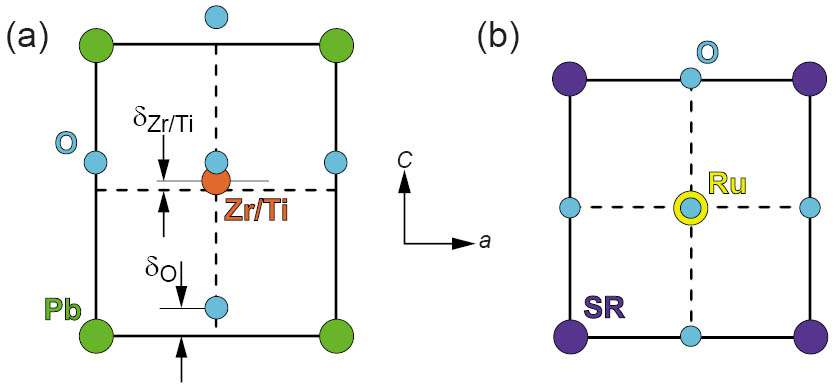
Figure 1: (a) Tetragonal PZT ferroelectric phase in a projection along the crystallographic b-axis. (b) Tetragonal centrosymmetric SRO.
Figure 2 shows a [010] HRTEM image of the interface of the PZT/SRO heterostructure recorded employing a value of underfocus which is close to Scherzer conditions. The contrast minima correspond to the position of the cation columns projected along the crystallographic [010] direction. The difference in image contrast between the two film layers allows the position of the interface to be located as denoted by a thick horizontal arrow. The surface of the PZT layer (not visible in the image) is parallel to the SRO/PZT interface, and as measured in the image the thickness of the PZT layer is about 8 nm.
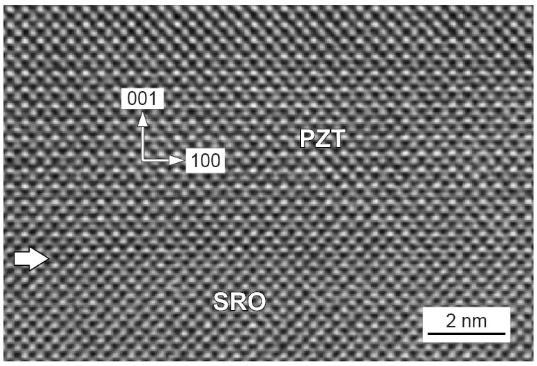
Figure 2: [010] HRTEM image of the PZT/SRO heterostructure The thick arrow denotes the horizontal interface between the PZT and the SRO film layers.
In order to map local polarization in the film, which is the result of relative displacements of ions as shown in Figure 1, the image of Figure 2 is quantified. The positions of atoms are determined by performing an iterative procedure in which the imaging parameters and structure model are systematically varied until a stable best fit of the calculated contrast distribution to the experimental intensity data for the SRO and PZT layers is achieved [1]. We note that we shall only deal with shifts of atomic positions as a function of increasing distance from the SRO/PZT interface plane. Therefore, for a certain distance from the interface, we calculate a mean value by taking the average of the contrast minimum position data over 42 unit cells (16.4 nm) parallel to the interface. Figure 3a shows the experimental image obtained by this type of averaging. It can be compared with the image in Figure 3b calculated on the basis of the final model of PZT/SRO and the optimum imaging parameters.
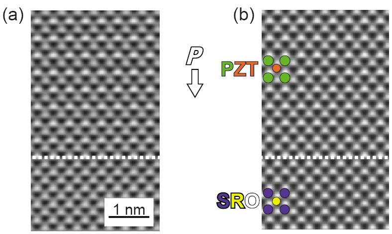
Figure 3: (a) Image obtained from the experimental image of Figure 2 by averaging the intensity over 42 unit cells. (b) The image calculated on the basis of final structure model. The polarization direction of the PZT film is shown by an arrow P.
In Figure 4a we present the results of measurements for the c-axis and a-axis lattice parameter. We find that the c-axis lattice parameter c of the PZT layer increases gradually with increasing distance from the interface reaching a maximum at a distance of about 4 unit cells from the interface, i.e. in the middle of the film. Here c reaches a value of 0.422 nm. Figure 4b shows the displacements δZr/Ti and δO of the Zr/Ti and O atoms, respectively, as a function of the unit cell position from the interface. For comparison, the shifts (open symbols) of the Ti and oxygen atoms in the bulk PTO ferroelectric phase are also displayed. Interestingly, the relative shifts of the atoms which result in the polarization of the ferroelectric phase are much smaller in the thin film system than in the bulk crystal. The change of the atomic displacements shows essentially the same behaviour as the c-axis lattice parameter.
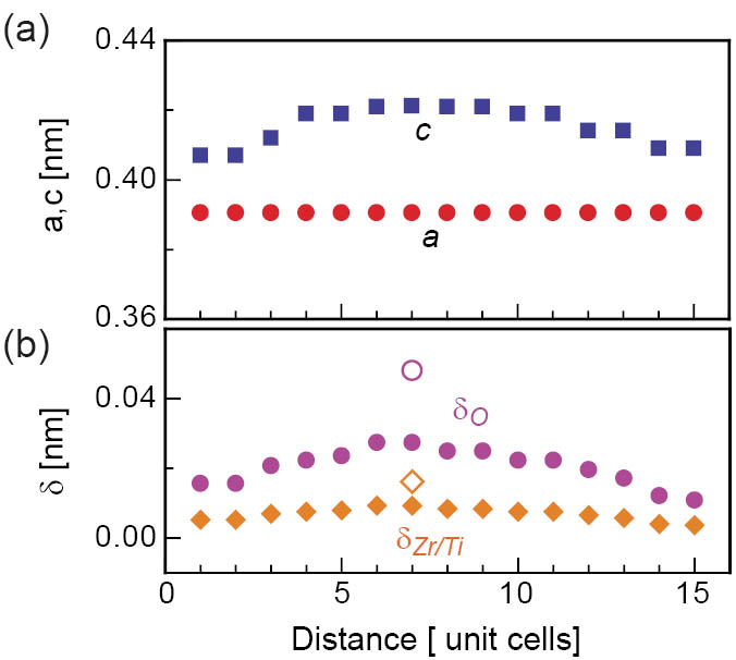
Figure 4: The c- and a-axis parameters (a) and the displacement parameters δZr/Ti and δO of the Zr/Ti and O atoms (b) as a function of the unit cell position from the interface.
In Figure 5 we show the spontaneous polarization, PS (full red circles) as a function of the distance from the interface calculated on the basis of the determined atomic displacements and the effective charge values of ions for PTO given in ref 2. The dotted line in the left part indicates the SRO/PZT interface position. As one progresses from the centre of the PZT film towards the interface or the film surface the value of PS decreases. This provides direct evidence for the fact that an interfacial layer with reduced polarization is formed in PZT. On the other hand, this behaviour supports the theoretical picture of surface-induced suppression of polarization based on a phenomenological theory. The blue dashed curve is calculated following the Kretschmer-Binder model [3] for a system of an 8-nm-thick ferroelectric sandwiched between metallic electrodes. Extrapolating the tangent at the interface we obtain values for the so-called extrapolation length on the PZT/SRO interface λ ≈ 1.9 nm and the bulk correlation length ξ ≈ 3.35 nm. We note that in the area close to the film surface the observed decrease in the polarization is much stronger in comparison with that at the PZT/SRO interface. This indicates that the local polarization is strongly influenced by the electrical boundary conditions. From our data, an averaged value of the spontaneous polarization ̅PS over a film thickness is estimated as 40 μC/cm2 for an 8-nm-thick film. This value for Δ̅PS ( = 2̅PS) fits quite well with the experimental data of about 70 ± 5 μC/cm2 [4].
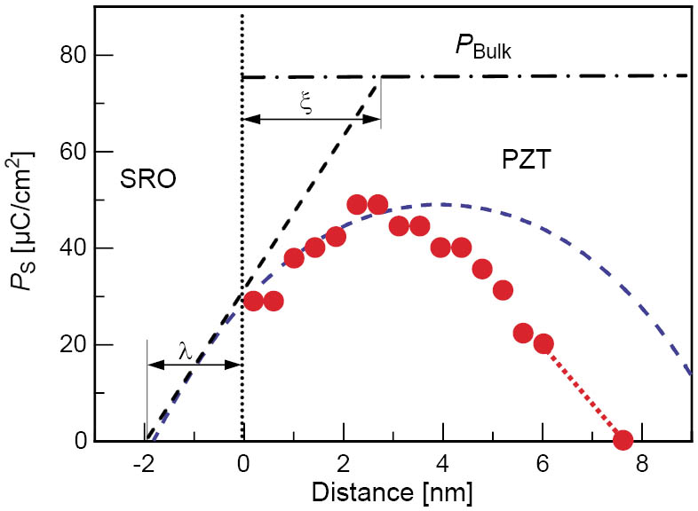
Figure 5: Spontaneous polarization, PS, calculated on the basis of the atomic shifts determined. The blue dashed-line curve is calculated for a system of an 8-nm ferroelectric layer sandwiched between metallic electrodes based on the Kretschmer-Binder model.
From our analysis, two key results are evident. Firstly, the displacements of the Zr/Ti and oxygen atoms decrease almost linearly from the film interior to the interface. It ca imagine that as the film thickness is increased, the effect of the interface becomes weaker and weaker. This observation corresponds to the increase in switchable polarization with increasing film thickness. A second important result is the evidence for smaller displacements of the Zr/Ti atoms from the positions of centrosymmetry in the film interior where the c-axis parameter is larger in comparison with the crystal data for the PTO ferroelectric phase. These smaller displacements are expected to lead to lower polarization. One possible role may be the kinetics of the growth process.
C. L. Jia, V. Nagarajan1, J. Q. He, L. Houben, T. Zhao2, R. Ramesh2, K. Urban, R. Waser
CNI – Center of Nanoelectronic Systems for Information Technology (IFF-6, IFF-8)
and Ernst Ruska-Centre for Microscopy and Spectroscopy with Electrons (ER-C)
1School of Materials Science and Engineering, University of New South Wales, Sydney NSW, Australia
2Dept of Materials Science and Dept of Physics, University of California, Berkeley, CA 94720, USA
Thickness Dependence of Intrinsic Dielectric Response and Apparent Interfacial Capacitance in Ferroelectric Thin Films
We studied theoretically the influence of the progressive strain relaxation and the depolarizing-field effect on the thickness dependence of the out-of-plane dielectric response of epitaxial ferroelectric thin films sandwiched between extended metal electrodes and compared it with the experimental data obtained for single-crystalline SrRuO3/Ba0.7Sr0.3TiO3/SrRuO3 and Pt /Ba0.7Sr0.3TiO3/SrRuO3 thin-film capacitors. The calculations show that the inverse of the measured capacitance varies with the film thickness almost linearly in the most part of the thickness range at the majority of temperatures. Extrapolation of this linear dependence to zero thickness usually gives considerable nonzero intercept even in the absence of nonferroelectric interfacial layers. Remarkably, such apparent “interfacial capacitance” may be strongly temperature dependent and becomes negative in a certain temperature range.
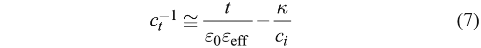
Pronounced thickness dependence of the physical properties of ferroelectric thin films is a severe obstacle for the application of these materials in electronic devices which meet the demands of the current trend for miniaturization. Experimentally, the inverse of the measured capacitance ct varies linearly with the film thickness. This observation led to a widely accepted interpretation of experimental data in terms of a “series capacitor model” (see expression in Figure 1). This model implies that the permittivity εb of the film interior and the interfacial capacitances ci1 and ci2 are thickness-independent quantities. This assumption, however, seems to be generally incorrect for real ferroelectric capacitors, because the experimentally determined ci values can be strongly temperature dependent and may even become negative (see Figure 1). This renders the interpretation of ci as an interface capacitance density questionable.
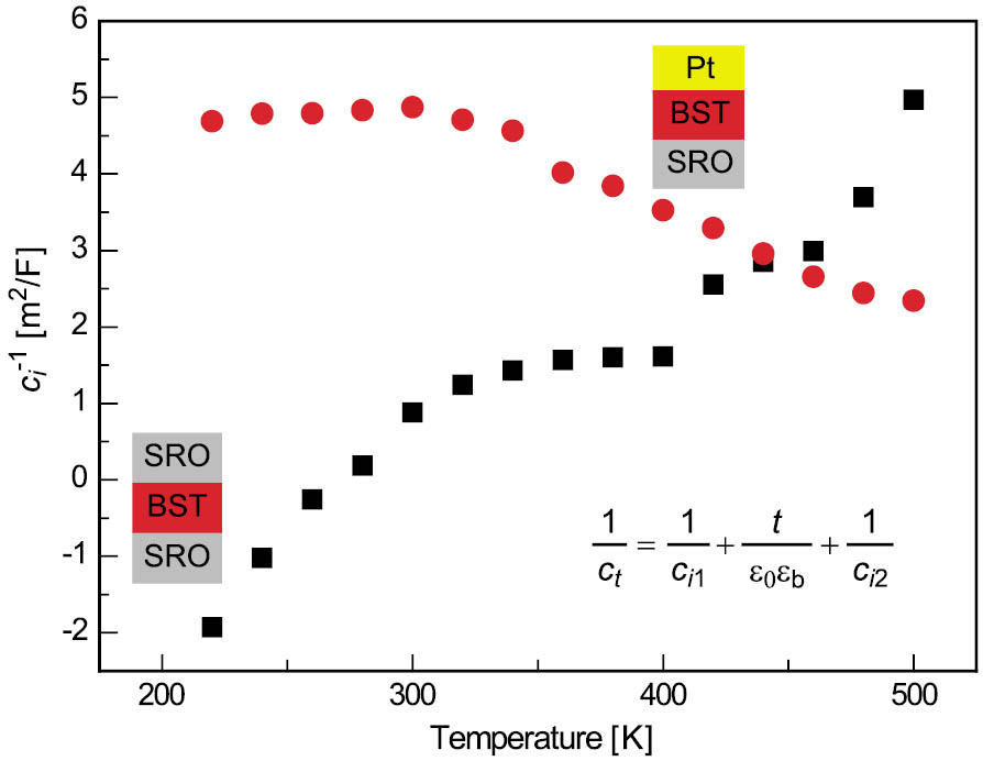
Figure 1: Equation according to the “series capacitor model”: εb = permittivity of the film interior, t = film thickness, and ci1 and ci2 = interface capacitance of two interfaces. Graphs: Temperature dependence of the intercept ct−1(t→0) extracted from the experimental data for Pt/Ba0.7Sr0.3TiO3/SrRuO3 and SrRuO3/Ba0.7Sr0.3TiO3/SrRuO3 capacitors [1].
We used a nonlinear thermodynamic theory to study in detail the influence of strain relaxation and depolarizing field on the thickness dependence of the small-signal dielectric response of ferroelectric capacitors compressively strained by a dissimilar cubic substrate and sandwiched between continuous metal electrodes.
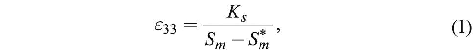
The strain effect on film permittivity is closely related to the strain-induced shift of the paraelectric to ferroelectric phase transition. Within the stability range of the paraelectric phase, the relative out-of-plane permittivity ε33 of an epitaxial film depends on the misfit strain Sm as
where Ks−1 > 0 is the strain sensitivity of the film reciprocal permittivity, and Sm* < Sm is the temperature dependent critical misfit strain [2]. The progressive strain relaxation caused by generation of misfit dislocations in films with thicknesses t exceeding the critical value tc results in the following thickness dependence of Sm:
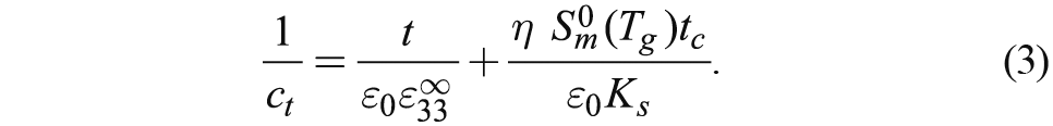
where Sm∞(T) represents the strain in a very thick epitaxial film (t ≫ tc) and η < 1 allows for the fact that usually the equilibrium dislocation density is not reached due to kinetic limitations. According to Eqs. (1) and (2), at t > tc the reciprocal capacitance varies with the film thickness as
It can be seen that the extrapolation of ct−1 to zero thickness gives a finite intercept caused by the strain relaxation. Remarkably, when the in-plane film strains at Tg are compressive (Sm0 < 0), the intercept ct−1(t→0)is negative.
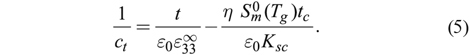
For epitaxial films in the ferroelectric state, we discuss the range of relatively large negative misfit strains, where the tetragonal c phase with the out-of-plane spontaneous polarization (P1 = P2 = 0, P3 ≠ 0) becomes energetically most favorable. Near the second-order phase transition, where the P4 approximation is valid, the dependence of the film permittivity ε33 on the misfit strain takes the form [1]
where Sm < Sm* and Ksc = Ks/2. The thickness dependence of reciprocal capacitance in the ferroelectric case becomes
It can be seen that the thickness-independent term in Equation (5) differs from that in Equation (3) by the opposite sign and by a two times larger magnitude. Since the c phase can form only at negative misfit strains [3], the strain Sm0(Tg) involved in Equation (5) usually must be negative. Therefore, in the ferroelectric regime the intercept ct−1(t→0) normally is expected to be positive. In summary, the strain effect leads to a change of sign of the intercept at the transition temperature.
We proceed now to the analysis of the influence of the depolarizing field on the dielectric response of a ferroelectric capacitor. This field appears when the polarization charges existing at the film surfaces are not perfectly compensated for by other charges. Since the electronic screening length in metals is finite, the depolarizing field may be significant even in short-circuited capacitors [4]. We model the ferroelectric/electrode interfaces by thin low-permittivity dielectric layers with a fixed thickness d ≪ t and permittivity εd. If variations of ferroelectric polarization near film surfaces are negligible, the above parameters can be evaluated as d = √εm lTF and εd = εm, where lTF and εm are the Thomas-Fermi screening length and the lattice dielectric constant of the electrode material, respectively.
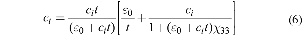
Assuming the film to be in a single-domain state, we can calculate the total capacitance density ct = ∂D3(V)/∂V as
[5] where χ33 = ∂E3/∂P3 represents the inverse susceptibility of the ferroelectric film in the capacitor, and ci = (1/2)ε0εd/d is the total capacitance density of two interfacial layers. The depolarizing field affects χ33 via suppression of the film out-of-plane polarization P3. Whereas ct−1(t) is linear in the P4 approximation, this dependence becomes nonlinear in the P6 and higher-order approximations. The numerical calculations, however, show that the nonlinearity is usually negligible when ct−1(t) is plotted over a limited thickness range only. Hence the thickness dependence of the reciprocal capacitance may be approximated by the relation
involving two fitting parameters, εeff and κ. Remarkably, the extrapolation to zero thickness gives a negative intercept equal to −κ/ci, which may significantly vary with the temperature.
For ferroelectric capacitors with film thicknesses outside the nanoscale range (t > tc) and imperfectly screening electrodes, the influence of both the strain relaxation and the depolarizing field has to be taken into account. We performed numerical calculations of ct−1(t) in the P8 approximation for BaTiO3 capacitors with two different interface capacitances ci. Nonlinearity of the dependence ct−1(t) was proved to be negligible at the majority of temperatures, and the intercept ct−1(t→0) was plotted as a function of temperature (see Figure 2). For both values of the interface capacitance, the intercept changes sign on crossing the phase transition region. In case of electrodes with good screening properties (ci = 1 F/m2), the strain effect dominates so that the intercept is positive at low temperatures and negative at high temperatures. For electrodes with poor screening ability (ci = 0.2 F/m2), the depolarizing-field effect overrides the influence of strain relaxation.
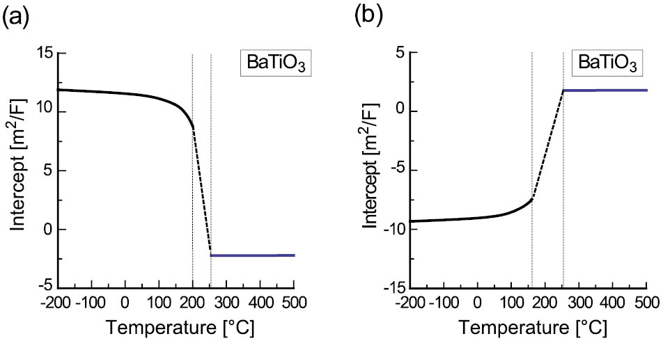
Figure 2: Temperature dependence of ct−1(t→0) calculated for BaTiO3 thin-film capacitors sandwiched between electrodes with different screening ability: (a) ci = 1 F/m2, (b) ci = 0.2 F/m2. We assumed Sm = −15 × 10−3, tc = 10 nm, η = 0.7, and ∂Sm/∂T = 4 × 10⁻⁶ K−1[5].
Thus, the observed two different types of the temperature dependence of the intercept, which are shown in Figure 1, can be qualitatively explained by our calculations.
- [1] R. Plonka, R. Dittmann, N. A. Pertsev, E. Vasco, and R. Waser, Appl. Phys. Lett. 86, 202908 (2005)
- [2] N. A. Pertsev, V. G. Koukhar, R. Waser, and S. Hoffmann, Appl. Phys. Lett. 77, 2596 (2000)
- [3] N. A. Pertsev, A. G. Zembilgotov, and A. K. Tagantsev, Phys. Rev. Lett. 80, 1988 (1998); V. G. Koukhar, N. A. Pertsev, and R. Waser, Phys. Rev. B 64, 214103 (2001)
- [4] R. R. Mehta, B. D. Silverman, and J. T. Jacobs, J. Appl. Phys. 44, 3379 (1973)
- [5] N. A. Pertsev, R. Dittmann, R. Plonka, and R. Waser, submitted to J. Appl. Phys.
N. A. Pertsev, R. Dittmann, R. Plonka, R. Waser
Nanotwins in BaTiO3 Thin Films
TASK
Ferroelectric BaTiO3 films epitaxially grown on insulating substrates like MgO are investigated for optical waveguides and electro-optic modulators while high-permittivity paraelectric BaTiO3-based thin films with a textured columnar morphology are studied for integrated capacitor and DRAM applications. Both, the electro-optic properties as well as the dielectric losses are strongly influenced by extrinsic defects. Within this project, the crystallographic types and densities of extended defects in BaTiO3 thin films were investigated.
APPROACH
The structure and configuration of {111} twins in polycrystalline BaTiO3 films prepared on platinum coated silicon wafers by pulsed laser ablation and chemical solution deposition were investigated by means of high-resolution transmission electron microscopy (HRTEM). The structure analysis was performed by image simulations.
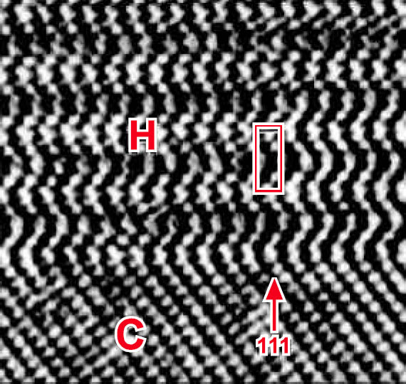
Figure 1: A HRTEM lattice image showing a local hexagonal structure (H) in the cubic BaTiO3 matrix (C), which is built up by an ordering of several nanotwin lamellae. A frame traces the unit cell of the hexagonal structure.
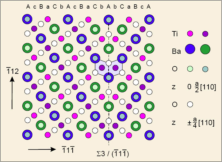
Figure 2: A [110] projection of the cubic BaTiO3 including a Σ = 3, (̅11̅1) twin boundary showing the stacking configuration of the Ti(̅11̅1) and BaO3(̅11̅1) atomic planes in the perfect structure and for the twin structure along the [̅11̅1] direction. The different symbols stand for different atoms at different height levels in the [110] direction. The shaded rhombuses show the projected oxygen octahedrons which share a face at the twin boundary (indicated by the broken line).
RESULTS
The HRTEM investigations show that the {111} twin boundaries represent the major type of defects in the polycrystalline BaTiO3 thin films. The number density of the twins in these films is high compared to bulk ceramics and the thickness of the twin lamallae is typically in the range of nanometers. In some grains, ordering of these nanotwins gives rise to a local structure which resembles that of the hexagonal phase. In most cases the twin lamellae extend to penetrate the whole grain. Based on the structure of very small twins (less than 1 nm in thickness) it can be shown that the formation of a {111} twin from dissociation of an a <111> edge dislocation is one of the mechanisms of twin formation in polycrystalline BaTiO3 films.
S. Hoffmann, C. L. Jia
Curie-Weiss Behavior of (Ba1-xSrx)TiO3 Thin Films
TASK
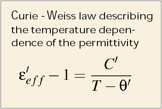
The permittivity of superparaelectric and paraelectric thin films is distinctly lower than the permittivity of conventional bulk ceramics of the same composition. In order to reveal the physical nature of this difference, an analysis of the Curie-Weiss behavior of the temperature dependence of the permittivity has been performed.
APPROACH
Ba1-xSrx)TiO3 thin films which were deposited on Pt coated Si wafers by CSD technique typically exhibit a polycrystalline microstructure. The dielectric properties of these films are controlled by the mean grain size, the degree of orientation, the porosity, and thermal stress effects. The morphological properties are controlled by the thin film deposition procedure and the substrate properties while the stress is caused by different thermal expansion coefficients of the film and the substrate. The temperature dependence of the permittivity of (Ba1-xSrx)TiO3 thin films was analyzed with respect to porosity effects by means of a mixing rule theory for a two component system.
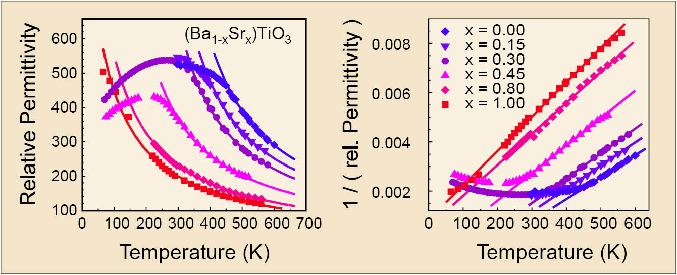
Figure 1: Temperature dependence of the permittivity and reciprocal permittivity, respectively, of (Ba1-xSrx)TiO3 thin films. Impedance measurements were performed on Si/SiO2/ZrO2/Pt/270 nm (Ba1-xSrx)TiO3/Pt structures at 10 kHz with a 0.1 Vrms signal. All compositions show a Curie-Weiss like behavior at high temperatures with a Curie-temperature shifted to lower values compared to bulk data.
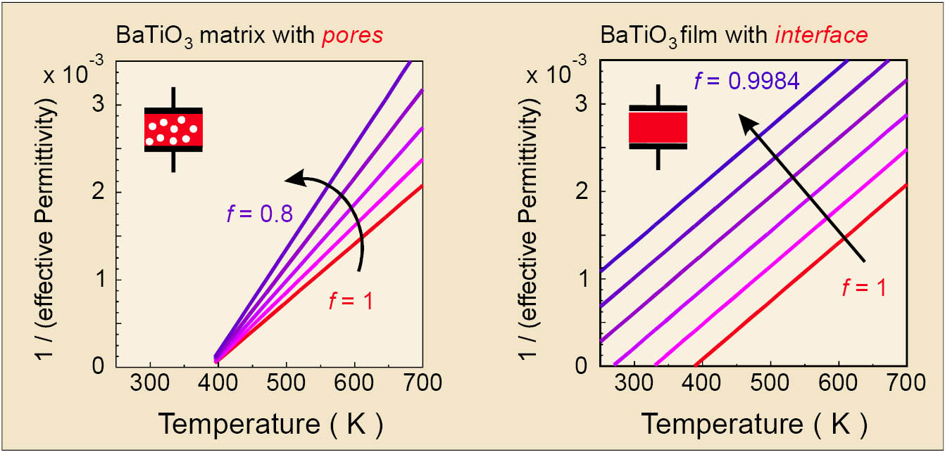
Figure 2: Calculated reciprocal permittivity vs. temperature for a two component system of BaTiO3 and air (ε′ = 1) mixed homogeneously (left) and for a layered stack of BaTiO3 and air (ε′ = 1) (right), respectively.
RESULTS
All (Ba1-xSrx)TiO3 thin films under investigation exhibit a Curie-Weiss behavior of the temperature dependent permittivity above the phase transition temperature. In comparison to bulk ceramics, the thin films exhibit a strong decrease of the Curie-temperature while the Curie-constant is only slightly changed. By simulating the influence of a second phase with low permittivity on the effective Curie-Weiss behavior of the thin films different mixing rules were applied for the system titanate/low-k phase. The results show clearly that the observed shift of the Curie-temperature can only be explained by a low permittivity interfacial layer between the thin film and the electrode. This interface may be caused by either an intrinsic (phononic) dead layer and/or interfacial porosity effects, stress effects or stoichiometry effects.
S. Hoffmann
Imprint in ferroelectric thin films: Interface-Screening-Model
Task
Imprint is besides fatigue and retention loss one of the most important failure mechanism of ferroelectric thin films in view of memory applications. Imprint manifests itself as a shift of the P-V hysteresis loop on the voltage axis. In literature, several models have been proposed as an explanation for the imprint effect. However, these literature models fail to explain the impact of at least one essential experimental parameter on imprint. Hence, a new model is proposed which allows a quantitative description of the imprint effect for the most important experimental parameters.
Approach
A detailed investigation has been performed in order to check the validity of existing literature models explaining the imprint effect. Up to now, the most likely imprint scenarios were described by the defect dipole alignment model and the bulk screening model. However, in ferroelectric thin films these models fail to predict the enhancement of imprint due to illumination, the independence of donor as well as of acceptor doping (defect dipole alignment model) and the enhancement of imprint caused by an externally applied bias (bulk screening model). Based on a comprehensive experimental investigation the Interface-Screening-Model is introduced which allows a quantitative description of imprint in ferroelectric thin films.
Results
In ferroelectric materials many indications about an thin surface layer can be found in which the spontaneous polarization is suppressed. A fact which causes a strong electric field Eif within the surface layer (Figure 1). Eif depends linearly on the ferroelectric polarization and reciprocally on the capacitance Cif of the thin surface layer. In the course of aging the electric field Eif causes the transport of electronic charges within the surface layer according to a Frenkel-Poole type emission (Figure 2). These charges become then trapped at the surface-layer-ferroelectric-interface. Hence, Eif becomes gradually screened by the trapped charges.
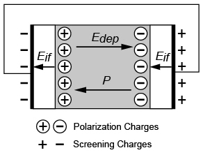
Figure 1: Sketch of the bulk screening model with the driving force EDep and Interface screening model: Enlargement of the interfacial region showing the driving force of the interface screening model Eif in the surface layer.
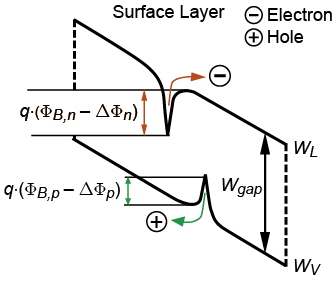
Figure 2: Sketch of the Frenkel-Poole emission of trapped electrons and holes. An electric field leads to a barrier lowering by δΦ{p} for holes and δΦ{n} for electrons.
With this model, the enhancement of illumination as well as the independence of doping can be qualitatively understood since this mechanism is of electronic origin. Also the enhancement of an externally applied bias in the direction of the polarization can be explained since the driving force and the external bias point in the same direction.
Implementing this mechanism into a numerical simulation provides even the possibility of a comparison between experimental and simulation results. With the Interface-Screening-Model, the time, thickness (Figure 3), and temperature dependence (Figure 4) as well as the improvement due to the use of oxide electrodes (Figure 5) can be quantitatively explained.
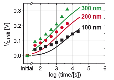
Figure 3: Imprint measurements performed at different tthicknesses (symbols, PZT, 20:80) and the corresponding numerical simulations according to the Frenkel-Poole mechanism (lines).
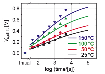
Figure 4: Imprint measurements performed at four different temperatures (symbols, PZT, 20:80, 200 nm) and the corresponding numerical simulations according to the Frenkel-Poole mechanism (lines).
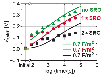
Figure 5: Imprint measurements performed at different electrode-ferroelectric systems (symbols, PZT, 20:80, 200 nm) and the corresponding numerical simulations based on different interface capacities (lines).
M. Grossmann
Size effect on the crystallographic structure of KNaNb2O6
Task
In recent years, lead free piezoelectric ceramics such as KNaNb2O6 (KNN) are gaining increasingly importance. Conventional powders of this system obtained by preparation routes based on solid state reaction, however, are known to be inherently difficult to sinter to full density. Therefore ultrafine and thus highly sinter active powders synthesized by chemical means are required. The crystallographic structures of nanocrystalline and submicron KNN are of fundamental significance because these determine the functional properties and in particular piezoelectric response. The aim of the present study is to investigate the size effect on the crystallographic structure in KNN.
Approach
Stoichiometric KNN powder was prepared through the hydrolysis of mixed K-, Na-, and Nb- ethoxides using a water in oil microemulsion as reaction medium. In order to remove organic impurities and to promote crystallization, the powder was annealed at various temperatures. X-ray powder diffraction (XRPD) and Raman spectroscopy, which detects even very small lattice distortion, were combined to investigate the size-induced phase transformation.
Results
KNN raw powder consisted of the particles with an average size of ca. 30 nm obtained after synthesis was amorphous. Upon annealing at temperatures above 600 to 1000 °C, no amorphous phase was detected as second phase any more. The most drastic change in particle size and shape observed for the powders annealed at 625 and 700 °C.
Above a particle size of 200 nm, the XRPD patterns could be refined as a monoclinic phase (M-type structure). Below 200 nm, a new KNN polymorph with triclinic symmetry was found.
Three different space groups P2/m (C2h1), P2 (C21) and Pm (CS1) are considered to be possible for the M-type structure based on XRD extinction rules. Raman results confine P2 and Pm which have 4A + 8B and 8A′ + 4A′′ Raman active normal modes as the space groups for the M-type structure. On the other hand, two space groups P1 (C11) and P-1 (Ci1) in the triclinic symmetry which have the Raman active normal modes 27A and 6Ag, respectively, are possible for the T-type modification. The Raman spectrum of the T-type polymorph showed extensive broadenings of the bands and contains more than 12 bands as deduced from the curve analysis. Therefore, space group P1 is believed to be more suitable for the description of the T-type polymorph. P2, Pm and P1 structures have no inversion center. Further all these structures have polarity, that is, spontaneous polarization. Consequently all these structures have piezoelectric and pyroelectric properties.
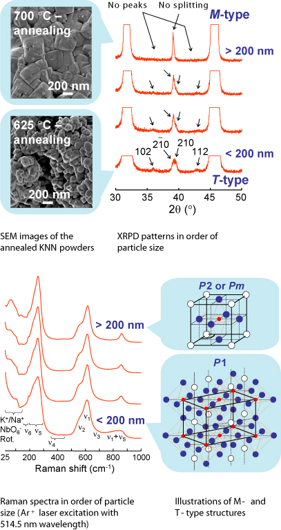
Figure 1: Quantum efficiency of an amorphous silicon thin film solar cell co-deposited on smooth and texture-etched ZnO:Al coated glass substrate. The enhancement of the long wavelength quantum efficiency by light trapping is schematically illustrated by the HRSEM cross-section micrograph of an amorphous silicon thin film solar cell on textured TCO.
Y. Shiratori, C. Pithan, A. Magrez (now at: EPFL, Switzerland)