nanoscale electron transfer - towards redox-based Tera-bit memories
In a range of oxides, for example transition metal oxides, field-induced ion migration on the nanoscale takes place at relatively low temperatures. This ion migration is typically accompanied by redox reactions at the electrode interface and electron transfer reactions. In the case of the migration of oxygen ions, the redox reaction occurs in the transition metal cation sublattice and often leads to insulator-metal transitions. The formation and dissolution of electron conducting channels may possibly be used for non-volatile resistive memories with integration densities up to Terabits per sqcm. Our research aims at the elucidation of the molecular structure of fast ion migration paths, the formation of space charge regions, details of the redox reaction in the oxide, and a microscopic view of the charge transfer reaction at the electrode interface. This research field is highly interdisciplinary involving solid-state and surface physics, electronic engineering as well as nanotechnology.
Origin of the Nonlinear Switching Kinetics and Scaling Studies of Valence Change Memory Cells
Experimental pulse length-pulse voltage studies of SrTiO3 memristive cells which reveal nonlinearities in the switching kinetics of more than nine orders of magnitude were performed. The experimental results are interpreted using an electro-thermal 2D finite element model. The nonlinearity arises from a temperature increase in a few nanometer thick disc-shaped region at the Ti electrode and a corresponding exponential increase in oxygen vacancy mobility. Our model fully reproduces the experimental data and it provides essential design rules for optimizing the cell concept of valence change memories. The model is generic in nature: it is applicable to all those oxides which become n-conducting upon chemical reduction and which show significant ion conductivity at elevated temperatures.
Valence change memory (VCM) cells are a promising candidate for next generation non-volatile, high speed and highly scalable memory cells [1,2]. Particularly, a huge nonlinearity in the switching kinetics is needed to meet the demands posed by the voltage-time dilemma [2]. It is widely accepted that the drift of oxygen vacancies on the nanoscale and a subsequent electrochemical redox process are responsible for the VCM effect . Hereby, the movement of oxygen vacancies due to ion hopping is the limiting factor in the switching process. The mobility of ions can be either field accelerated or temperature activated. But, a detailed investigation of the dominating process has not been shown yet. Herein, we report on experimental switching kinetics studies on SrTiO3 based VCM cells. The experimental results are interpreted using an electro-thermal 2D finite element model which allows for discriminating between the field and temperature contribution to the ion mobility enhancement. This electro-thermal model is subsequently employed to investigate the scaling potential of VCM cells.
The SrTiO3 thin films with 1 at% Fe-doping of 50 nm thickness were grown by pulsed laser deposition (PLD) on (100)-oriented 1 at% Nb-doped SrTiO3 (Nb:STO) single crystals serving both as substrate and bottom electrode. Subsequently, circular top electrodes of 50 µm diameter were prepared by magnetron sputtering of Pt (50 nm)-covered Ti (50 nm) through a shadow mask. By a wet-etching step using buffered HF solution a part of the bottom electrode was exposed. Al wire bonding of the bottom electrode was used to achieve an ohmic contact. An initial quasistatic I-V sweep was used to electroform the VCM cell.
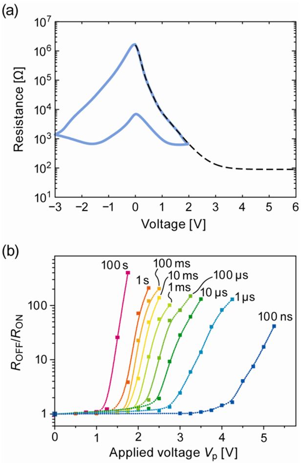
Figure 1: (a) R-V characteristic of a measured cell (blue curve) and in the simulation (black dashed curve). (b) SET switching dynamics of the corresponding sample for different pulse amplitudes and pulse widths, shown as the ROFF/RON ratio as a function of the applied voltage amplitude of the pulse and the pulse duration. (Redrawn from [3])
The fabricated VCM cells were electrically characterized by performing quasistatic I-V sweeps as well as by defined voltage pulses. Thereby, the voltage was always applied to the top electrode. The measured quasistatic R-V characteristic is shown in Figure 1a. Apparently, the low resistive state (ON state) and the high resistive state (OFF state) exhibit a nonlinear voltage dependence. A quasistatic resistance ratio ROFF/RON > 100 is observed for moderate SET and RESET voltages of 2 V and -3 V, respectively. Pulse measurements with a pulse duration Δtp ranging from 100 ns to 100 s and a pulse amplitude Vp ranging from 0.5-5 V were performed. Before and after a SET voltage pulse, the cell resistance was measured quasistatically to determine the resistance change. The cell was subsequently RESET to its initial OFF state using a quasistatic I-V sweep. Figure 1b depicts the resulting resistance change. A highly nonlinear switching kinetics is visible. Changing Vp by a factor of 5 leads to a change of 9 orders of magnitude in the Δtp required to SET the cell.
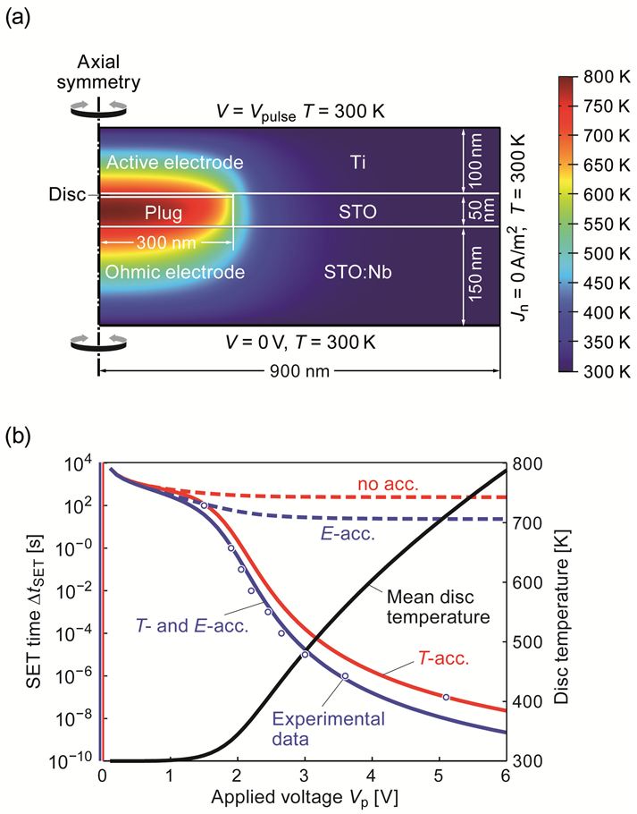
Figure 2: (a) Cross section of the simulated cell. The temperature distribution for Vp = 5 V is shown in color. (b) Calculated SET time depending on the applied voltage for the four different cases in red and blue. The black line corresponds to the mean disc temperature used for the calculations. The experimental data are extracted from Figure 1(b) for a resistance ratio ROFF/RON = 30 and shown as open circles.(Redrawn from [3])
To interpret the experimental data we consider a 2D axisymmetric finite element simulation model of the VCM cell (see Figure 2(a)). The simulated cell comprises an n-conducting cylindrical region ("plug") grown during electroforming in the SrTiO3 film and a disc shaped region at the top electrode interface ("disc"). The conductivity in the disc region is fitted so that the experimental R-V characteristic is obtained (cf. Figure 1a). The movement of oxygen vacancies through this interfacial disc region triggers the switching event. The SET time can thus be estimated from the disc thickness and the drift velocity of oxygen vacancies as ΔtSET = ldisc/vdrift. The drift velocity is calculated according to the Mott-Gurney law of ion hopping as
Here, the activation energy ΔWA = 1.01 eV, the characteristic field E0 = 1 MV/cm, and Edisc = Vdisc/ldisc. Hence, the SET time depends on the volt drop across the disc Vdisc and the mean disc temperature T. These quantities are extracted from numerical FEM simulations of the field and temperature distribution with the VCM cell. For this, the heat equation is solved for along with the continuity equation [3].
Figure 2a shows the simulated temperature distribution for an applied voltage Vp = 5 V. Apparently, the highest temperature emerges in the disc region. The resulting SET times (T- and E-acc.) are depicted in Figure 2b along with the mean disc temperature and the experimental data. Here, it is discriminated between the contributions of the field acceleration (E-acc.), the temperature acceleration (T-acc.). For comparison the non accelerated case for a purely linear drift (no-acc.) is shown. A best fit to the experimental temperature is obtained for a combination of field and temperature acceleration. Evidently, the latter is the dominating factor in interpreting the origin of the nonlinear switching kinetics. It has been shown that for all reasonable alternative scenarios, either the fitting procedure fails dramatically or unphysical parameter values have to be used [3].
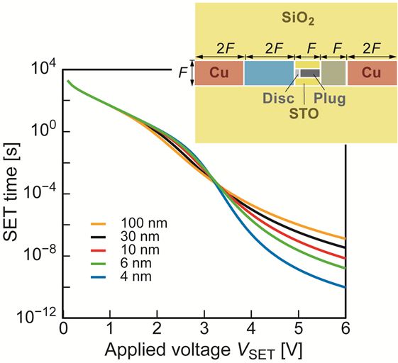
Figure 3: Calculated SET time depending on the applied voltage for temperature and field accelerated switching. The cell geometry is shown in the inset. The feature size F has been used as a parameter for the set of calculations. The disc thickness is 3 nm in all simulations and the diameter of the filament is 0.4 F.
To project the scaling potential of VCM cells the electro-thermal simulation model is applied to a nanosized axisymmetric VCM cell with an active electrode and an ohmic electrode as well as Cu interconnects and an adjacent SiO2 layer (see inset in Figure 3), while the dimensions scale with F. Figure 3 shows the calculated SET times depending on the applied voltage. Apparently, the switching speed for VSET > 3.5 V increases for smaller feature sizes F. This demonstrates that nanosized VCM cells are feasible.
- [1] R. Waser, R. Dittmann, G. Staikov, K. Szot, Adv. Mater. 21, 2632 (2009).
- [2] A. Sawa, Mater. Today, 11, 28 (2008).
- [3] S. Menzel, M. Waters, A. Marchewka, U. Böttger, R. Dittmann, R. Waser, Adv. Funct. Mater., 21, 4487, (2011).
S. Menzel, M. Waters, A. Marchewka, U. Böttger, R. Dittmann, R. Waser
Coexistence of filamentary and homogeneous resistive switching in Fe-doped SrTiO3 thin film devices
Resistance random access memory, short RRAM, has attracted considerable attention as a highly scalable future non-volatile memory concept. In the search for promising resistive switching oxide materials, special attention has to be paid to the scaling capabilities of the corresponding devices. The issue of scaling is strongly linked to the question of, whether the switching current is distributed homogeneously across the device area or localized to one or a few conducting filaments. While in the former case the scaling limit will be connected to the minimum device area, that guarantees sufficient switching currents for a reliable circuit operation, in the latter case, scaling might suffer from too large filament dimensions or their insufficient density and regularity within the material.
In this work, we used conductive AFM combined with a delamination technique to remove the top electrode of resistive switching Fe-doped SrTiO3 devices to gain insights into the nanoscale current distribution of formed and switched devices beneath the Pt top electrode[1],[2],[3]. The different approaches are sketched in Figure 1.
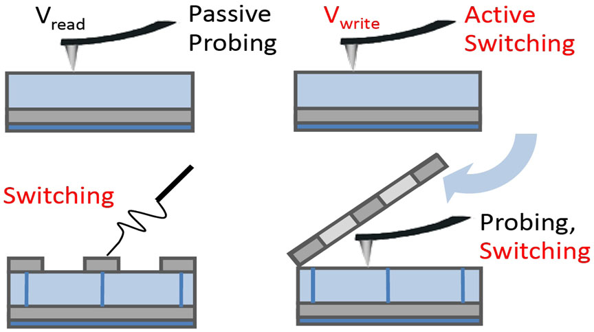
Figure 1: Illustration of the different approaches for switching and probing of resistive switching thin films and devices.
The current-voltage (I-V) characteristic of a Pt/ 500 nm SrTiO3(Fe) /Nb:SrTiO3 MIM-device after an initial electroforming process[4] is shown in Figure 2a. Starting at 0 V a stable resistive switching hysteresis, shown in green, is reached (1-2-3-4-1). In the following we call the “sense of rotation” or switching polarity of this curve “counter eightwise” polarity. If, however, the sample is swept further down to -3.5 V (curved orange arrow), a higher resistance state is reached. Keeping this higher negative voltage amplitude, a stable second type of switching can be achieved, shown in orange (1-5-6-4-1) showing an “eightwise” polarity. Both types of switching occur in the same pad. A repeatable change between both curves can be induced by adjusting the negative voltage amplitude back and forth again. This peculiar I-V behavior is very reproducible and can be observed on all of our samples as well as in related systems [5].
Both types of switching exhibit different electrode area scaling behavior: the “counter eightwise” switching type shows no discernable junction size dependence, hinting at a filamentary switching nature. Using certain forming conditions, however, we were able to fabricate samples showing only the “eightwise” switching type. These samples exhibit a clear padsize dependence hinting at a more “homogeneous” underlying effect.
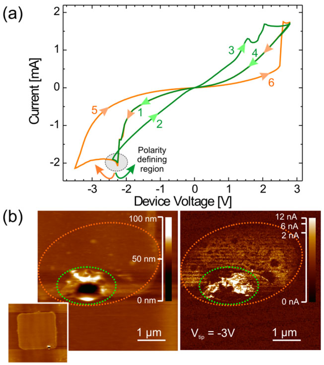
Figure 2: (a) I-V-characteristics of a Fe-doped SrTiO3 thin film. Two types of switching behaviour exhibiting opposite polarities can be seen in one and the same junction. (b) Conductive AFM topography and current image of a junction after electroforming and top electrode removal. The inset covers the whole junction area, while the main topography and current images are magnifications of the lower right part of the junction area. A well conducting crater (green) as well as a medium conducting region around the crater (orange) can be seen.
After forming and switching several junctions in the aforementioned way, we removed the top electrodes in a physical delamination process that ensures a complete but gentle Pt removal [2]. Figure 2b shows the topography and local current distribution of a junction determined by conductive-tip AFM (illustrated in Fig. 1). Most of the interface is smooth and has not been structurally altered by the electroforming step. Only a small region in the lower right part of the junction shows a roughly 1?m wide crater-like structure (marked by a green dashed line). In cooperation with the group of Prof. Mayer from the GFI at the RWTH Aachen we could prove that the defect density in this crater area is strongly increased. Photoemissions electron microscopy performed in cooperation with the group of Prof. Schneider (PGI-6) proved that Sr segregates to the surface in this area, leaving behind a Ti rich forming channel.
The conductivity of the formed junction is shown on the right hand side of Figure 2b. The crater itself is well conducting (marked in green) and a somewhat broadened area around the crater shows moderate conductivity (marked in orange). In a first step the conductive AFM tip was employed as a virtual electrode. The tip bias was biased with -5 V, scanned across the surface, and afterwards another readout image at -3 V was recorded. This treatment step results in a conductivity decrease of the area marked in orange (upper left part of Figure 3a). A second scan with a reversed tip bias of +5 V recovers the conductivity of that region (upper right part of Figure 3a). In fact, not only this initial region but the complete junction area within the scan range has been switched on. The polarity of this type of switching corresponds to the orange curve in Figure 2a.
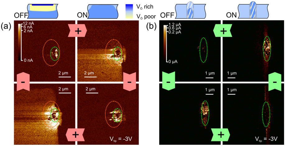
Figure 3: Tip induced resistive switching of a delaminated sample. (a) A positive voltage of +5 V will switch the broad area around the crater from Off to On state, while a negative voltage of -5 V switches it back from On to Off state. (b) Going to a higher current compliance allows resolving the crater itself. It can be switched as well (using tip voltages of +/- 6 V), but exhibits the opposite switching polarity.
The crater area itself can also be seen in these images (marked in green) and switched by the AFM tip as well (Figure 3b). The polarity of this type of switching is reversed compared to the previous case and corresponds to the green curve in Figure 2a. It is interesting to note that in this case only the crater region itself contributes to the switching, indicating a completely localized, filamentary process.
The correlation between the switching types observed in the MIM structure and the switchable regions seen under the AFM is demonstrated in Figure 4. Instead of using the AFM tip to switch a junction after delamination, two MIM structures have been switched within the “eightwise” polarity and set to the LRS and HRS state before delamination. After removal of the top electrode those samples were inserted into the AFM chamber and their conductivity images were compared. The junction that has been left in the LRS state (Figure 4a) shows both a conducting crater region and a conducting surrounding region. The junction that has been switched to the HRS state, however, lacks the conducting surrounding region (Figure 4b). Both this experiment as well as the AFM induced switching in Figure 3 therefore show, that resistive switching of the “eightwise” polarity takes place within an extended region surrounding the forming crater.
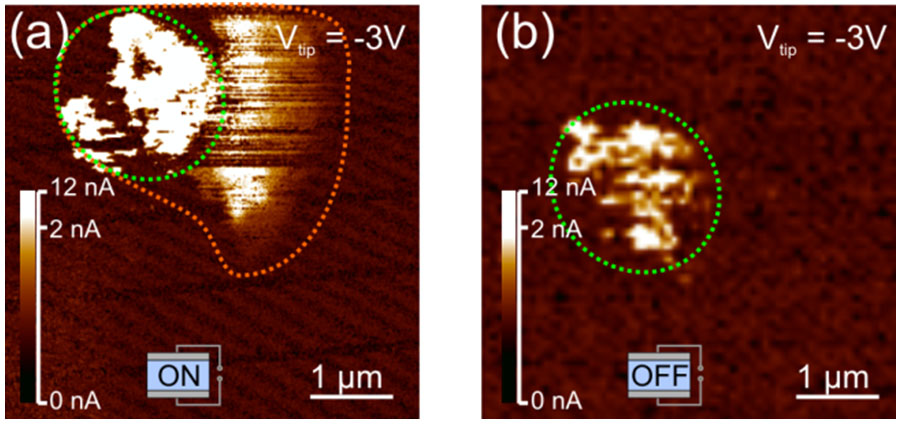
Figure 4: Conductive AFM current images of a junction that has been set to On state (a) and a junction that has been set to the Off state before delamination. A vanishing of the broadened conducting area around the crater due to the Off switching can be seen.
In conclusion, we have demonstrated that resistive switching in Fe-doped SrTiO3 thin films can be either confined to a single strong filament or distributed over larger areas beneath the electrode, in the ideal case the whole junction area. Both types of switching coexist in one and the same sample and exhibit the opposite switching polarity. We suggest allocating those two switching types to areas of different defect density beneath the same electrode. Concerning device scaling, these results imply that resistive switching in SrTiO3 thin films can in principle be extended over the whole junction area if the formation of thermally generated strong filaments is prevented during an appropriate electroforming process. However, whether filamentary or interface-type switching exhibits superior scaling capabilities has to be clarified in the future.
- [1] R. Muenstermann, T. Menke, R. Dittmann, and R. Waser, Adv. Mat. (2010).
- [2] R. Muenstermann, J. J. Yang, J. P. Strachan, G. Medeiros-Ribeiro, R. Dittmann, and R. Waser, Phys. Status Solidi-Rapid Res. Lett. 4, 16 (2010).
- [3] J. P. Strachan, J. J. Yang, R. Muenstermann, A. Scholl, G. Medeiros-Ribeiro, D. R. Stewart, and R. S. Williams, Nanotechnology 20, 485701 (2009).
- [4] T. Menke, R. Dittmann, P. Meuffels, K. Szot, and R. Waser, J. Appl. Phys. 106, 114507/1 (2009).
- [5] K. Shibuya, R. Dittmann, S. Mi, and R. Waser, Adv. Mater. 22, 411 (2010).
Ruth Muenstermann, Tobias Menke, Regina Dittmann, and Rainer Waser
Impact of defect distribution on resistive switching characteristics of Sr2TiO4 thin films
In this study, we will compare thin film samples with significant different defect structure and will thereby provide the experimental evidence of the correlation between defect density and switching properties. We will furthermore demonstrate the coexistence of two different switching characteristics with opposite polarity which can be reversible and controllable selected by the current load. We will clearly show that the two switching mechanisms are differently pronounced in different defect density and thickness regimes.
In order to develop resistive materials to applicable memory cells and to advance to the ultimate scaling limits for future ReRAM, deep understanding of switching mechanisms is indispensable. There exists a general agreement that the migration of oxygen vacancies under applied electric field plays an important role for resistive switching phenomena in oxides. Extended defects within the active thin film matrix have been claimed to play a crucial role, associated with the fact that oxygen-vacancy migration is significantly enhanced along extended defects.[1],[2] However, direct experimental demonstration of a correlation between defect distribution and switching properties has not been reported up to now. One of the reasons is the lack of materials with a well defined distribution of defects.
One advantage of using Sr2TiO4 thin films is the opportunity to control the defect density in the layer by the growth temperature.[3] Transmission electron microscopy (TEM) images of the films grown on nondoped SrTiO3 surfaces at 700 and 900 °C are presented in Figures 1 (a) and (b), respectively. The reduction of the thermal energy during the deposition resulted in a local cation nonstoichiometry and thereby in a high density of defects in the Sr2TiO4 layer. On the other hand, well-ordered layered sequences of Sr2TiO4 were formed at a higher growth temperature.
The as-grown insulating Sr2TiO4 films were transformed into a switchable state by performing an electroforming process.[2,4] Typical I-V characteristics of junctions with defective and nearly perfect Sr2TiO4 layers are shown in Figures 1 (c) and (d), respectively. In the case of the defective layer, large hysteresis windows especially in the reverse bias were observed in I-V cures, as shown in Figure 2 (c). On the other hand, little currents were seen in the reverse bias in the case of the less defective layer, as shown in Figure 2 (d). This was because the electroforming procedures could not be completed in the less defective films according to the less effective oxygen diffusion. Although the amount of oxygen vacancies was enough to obtain conductivity in the thin film, it was insufficient to overcome the Schottky-like barrier. Therefore a strong rectifying behavior was seen in Figure 2 (d). A high density of lattice defects was required for the completion of the conducting filaments.
Another intriguing feature was that the conductance in the incompletely formed interfaces as shown in Figure 2 (d) scales with the pad size of the top electrodes, denoting a homogeneous conduction.
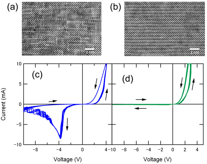
Figure 1: TEM images of Sr2TiO4 films grown on nondoped SrTiO3 substrates at (a) 700 °C and (b) 900 °C. I-V characteristics of the films grown on Nb-doped SrTiO3 surfaces at (c) 700 °C and (d) 900 °C, respectively. The thickness of the Sr2TiO4 layer was about 10 nm in both cases.
A typical feature of the Au/Sr2TiO4/Nb:SrTiO3 junctions with well pronounced hysteresis curves is that one can see two types of switching properties represented by the red and the blue curves in Fig. 2. The red curves were observed in the smaller voltage range of ±4 V. When a negative bias exceeded -4 V, negative differential resistance shows up and afterwards the switching polarity converts into the other direction (blue curve). The polarity of the red curve can be explained by oxygen-vacancy migration[1,2], judging from the resistance changes from LRS to HRS in the positive or the forward bias. The conductance of these switching curves was independent of the pad area, indicating a filamentary conduction.
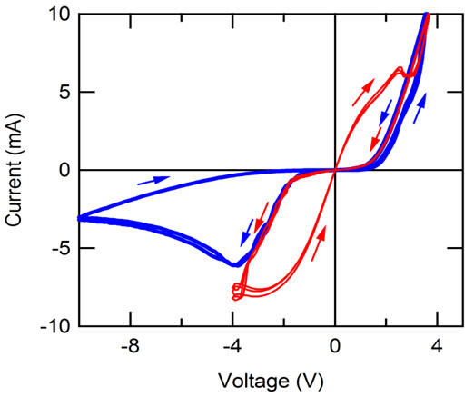
Figure 2: I-V curves of the junction with a 10-nm thick Sr2TiO4 layer grown at 700 °C
The other switching type (blue curve) showed a rectification behavior as the I-V curves of the pristine junction. The Schottky-like barrier seemed to be slightly modified during a voltage sweeping. This switching type is more stable than the other one and can exhibit area scaling depending on the used forming procedure. This behavior is similar to the interface-type switching reported by Sawa in metal/Nb-doped SrTiO3 single crystal structures without active layer.[5] Trapping and detrapping of electrons at oxygen vacancies in the interface has been suggested as possible switching mechanisms [4], but the exact origin will have to be investigated in future work.
The polarity conversion of these two switching types can be reversibly adjusted by the sweeping voltage range as shown in Fig. 2. The HRS of the red curve polarity corresponds to the LRS of the blue curve. The switching polarity conversion and the coexistence of the two switching types were exhibited above a film thickness of around 5 nm. Below the thickness only the “red-curve type” switching was observed. Figure 3 (a) is a schematic drawing of the switching polarities as functions of Sr2TiO4 layer thickness and growth temperature. It shows that both types of switching coexist in a broad range of conditions. Figure 3 (b) corresponds to Figure2 which shows I-V curves of the junction with a 10-nm thick Sr2TiO4 layer where both switching polarities were observed.
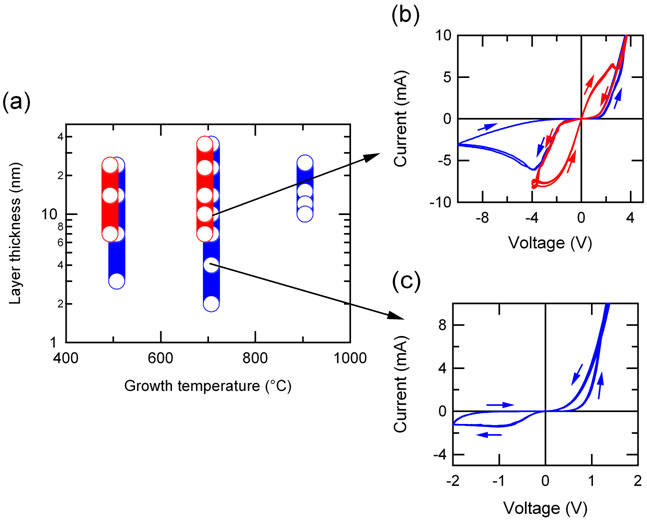
Figure 3: (a) A schematic drawing of switching polarities as functions of Sr2TiO4 layer thickness and growth temperature. I-V curves of the junction with (b) a 10-nm thick and (c) a 3.6-nm thick Sr2TiO4 layers grown at 700 °C.
When the layer is less defective, only the “blue-type curve” switching was seen, independent of the layer thickness. At ultrathin layers below 5 nm, the same polarity merely appeared even though the layers were defective, grown at lower temperatures. Typical I-V curves are presented in Figure 3 (c). Similar to Figure 1 (d), a rectification appeared but a relatively large reverse conductance showed up due to large tunneling currents through a very thin barrier. These results indicate that the “blue-curve type” switching emerges exactly at the interface while the switching process of the “red-curve type” polarity is more bulk-like due to the oxygen-vacancy migration along the extended defects.
In conclusions, we have demonstrated in Au/Sr2TiO4/Nb-doped SrTiO3 junctions the clear correlation between resistive switching properties and the density of defects which work as fast migration paths for oxygen vacancies. Therefore, the control of the distribution and the density of defects is a major task in terms of the fabrication of reproducible and scalable resistive switching devices. Furthermore, we observed the coexistence of two switching polarities which could be reversibly adjusted by the applied voltage range.
- [1] K. Szot et al., Nature Materials 5, 312 (2006)
- [2] R. Waser, R. Dittmann, G. Staikov, K. Szot, Advanced Materials 21, 1-32 (2009)
- [3] K. Shibuya, S. Mi, C.-L. Jia, P. Meuffels, R. Dittmann, Appl. Phys. Lett., 92, 241918 (2008)
- [4] K. Shibuya, R. Dittmann, S. Mi, R. Waser, Advanced Materials 22 , 411 (2010)
- [5] A. Sawa, Mater. Today 11, 28 (2008).
K. Shibuya, R. Dittmann, S. Mi, and R. Waser
Realization of Self-Assembled Arrays of Nanoscale Resistive Switching Blocks in Thin Films of Nb-Doped SrTiO3
We report on the realization of self-assembled arrays of nanoscale resistive switching blocks in epitaxial Nb-doped SrTiO3 thin films. These blocks have dimensions in the order of 30 nm and are embedded in an insulating matrix. They can be individually addressed by the tip of a conductive tip atomic force microscope and reversibly switched between a high and a low resistance state reaching an Roff to Ron ratio of up to 50. Scanning micrometer-scale areas with an appropriately biased tip in terms of voltage amplitude and polarity, all blocks within the scanned area can be switched between the two resistive states. We suggest a connection between these nanoscale switching blocks and defect-rich nanoclusters which were detected with high resolution transmission electron microscopy.
Searching for new concepts of non-volatile resistive memory devices an upsurge of interest in thin perovskite films as resistive switching layers has arisen ever since the discovery of an electric field induced resistance change in manganites and titanates as well as zirconates [1, 2]. For undoped SrTiO3 it was shown that the switching occurs along crystalline defects which extend through the sample and form a network of nanometer-sized filamentary conduction paths [3, 4]. This makes SrTiO3 a very promising candidate for a non-volatile memory in the terabit regime. Doping SrTiO3 with transition metals improves the stability of the resistive switching and may be a tool to influence the extension and the local distribution of switching units in SrTiO3 thin films. In this work Nb-doped SrTiO3 thin films are therefore investigated with a conductive tip atomic force microscope (LC-AFM). We explore the local current distribution and the arrangement of intrinsic nanoscale switching units of these films and relate it to the microstructure determined by high resolution transmission electron microscopy (HR-TEM).
Thin films were prepared by pulsed laser deposition (PLD) employing a KrF excimer laser (λ = 248 nm) with an energy density of 5 J/cm2 at a frequency of 10 Hz. A SrTiO3 target with a Nb-concentration of 1 wt% and commercially available NdGaO3(110) substrates were used. The substrate temperature was set to 700 °C. According to a background pressure of 1.2 × 10⁻⁵ mbar the oxygen partial pressure during deposition was estimated to be lower than 10−6 mbar. In order to investigate the local nature of the conductivity and the switching behaviour of the samples we performed LC-AFM measurements of all films. All measurements were carried out with a Jeol JSPM 4210 microscope under vacuum conditions with a background pressure of 10−5 mbar employing a PtIr-coated AFM tip.
The LC-AFM topography image and the corresponding local current distribution of a 1 wt% Nb doped SrTiO3 film is shown in Figure 1. The images were recorded with a negatively biased tip (Vtip = −3 V). The surface exhibits a hilly morphology (Figure 1a) and is covered with little protrusions. These protrusions correspond directly to roughly 30 nm wide circular spots in the current image (Figure 1b): the centre of each protrusion is conductive, while the boundaries are almost non-conductive. This correlation becomes particularly clear by comparing two linescans drawn at the same place in the topography and the current image respectively (Figure 1c). While similarly correlated systems described in the literature exhibit very irregular patterns, in our case the protrusions form an almost well ordered array of conducting spots.
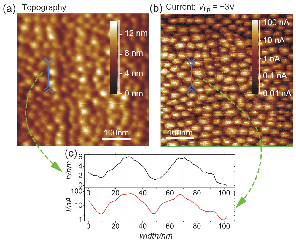
Figure 1: Part a and b show LC-AFM images of a Nb-doped SrTiO3 thin film. The surface of the film consists of protrusions with a conductive centre and practically non-conductive boundaries (part c) forming an array of conductive spots.
By applying an external voltage between the tip and the sample it is possible to change the resistance of these conducting spots, if the measurement is carried out under vacuum conditions. The central part of Figure 2 shows an I-V curve of a typical single conducting spot (indicated by the white dashed circle), which was recorded by placing the AFM tip over the spot and varying the applied voltage. The I-V curve has a clear hysteresis and shows a bipolar switching behaviour with an Roff to Ron ratio of up to 50. The current compliance is instrumentally limited to 1 μA. Stable switching curves can be recorded as long as the tip has not drifted away from the conducting spot. The switching behaviour can be reproduced for a large amount of conducting spots by scanning the positively (Vtip ≥ 2 V) or negatively (Vtip ≤ −3 V) biased tip over a defined area of the sample: all four current distribution images in the outer parts of Figure 2 are recorded with a tip voltage of −1 V. While in Figure 2a all spots inside the inner square are conductive, a scan over the area of the green dashed square with a negative tip voltage of at least −3 V switches all spots inside the scan area “off” (Figure 2b). A subsequent scan with a positive tip voltage of at least +2 V recovers the conductivity of the previously switched “off” spots (Figure 2c), while yet another scan with −3 V switches them “off” again (Figure 2d). In summary, it is possible to switch each of the 30 nm wide spots individually between two different resistance states.
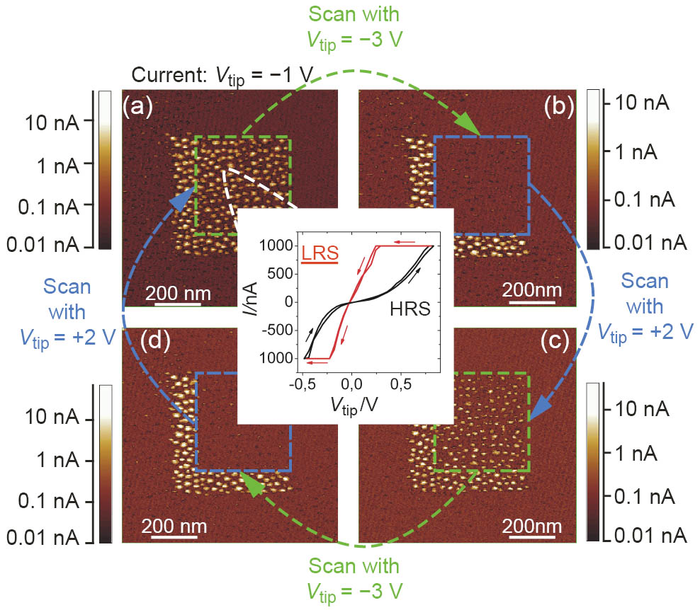
Figure 2: Reversible resistive switching in Nb-doped SrTiO3 deposited under low oxygen pressure. The current images show an array of conducting spots which can be switched between two different resistance states.
This switching behaviour is consistent with the current image in Figure 1b which was recorded with a negative tip voltage of −3 V while switching the scanned area “off”: The scan with the switching voltage of −3 V itself still shows the high conductivity of the low resistance state, while any following scan shows the almost non-conductive surface of the high resistance state.
In order to understand the microstructure of the film and thus the structural nature of the protrusions or the conducting spots, HR-TEM measurements of a Nb-doped SrTiO3 film grown under low oxygen pressure have been performed. They show that the film is grown coherently on the substrate without any misfit dislocations at the interface. It contains however a high density of defect-rich clusters with dimensions between 2 and 20 nm (Figure 3). Lattice defects and lattice distortion are detectable within these clusters.
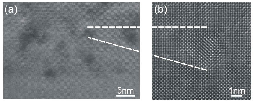
Figure 3: HR-TEM investigations reveal defect-rich clusters embedded in the matrix of the film. Part a shows a low magnification out-of-plane lattice image with several clusters, while part b shows a higher magnification of a single cluster.
Summarizing the TEM and LC-AFM results for our films, we see a structural inhomogeneity with lattice-distorted and defect-rich nanoclusters which have diameters in the range from 2 nm to 20 nm. Moreover the measurements show an electrical inhomogeneity with well conducting spots with diameters of approximately 30 nm. We assume a connection between the nanoclusters and the conducting spots because of their similar size and distribution although the exact nature of this correlation is not yet completely clear. Since the oxygen partial pressure has a major influence on the electrical measurements and since switching is only observable under vacuum conditions, we assume, that the switching process in Nb-doped SrTiO3 can be explained by a local oxidation and reduction along a network of electrically connected, defect-rich nanoclusters. More experimental evidence is however necessary to either confirm or disprove this assumption.
In summary, we have succeeded in fabricating regular arrays of 30 nm wide resistive switching blocks in Nb-doped SrTiO3 thin films, which can be switched between two different resistance states by applying an external voltage. We attribute these resistive switching blocks to the specific defect structure of our thin films.
This work was financially supported by Intel Inc., Santa Clara.
- [1] Y. Watanabe, J. G. Bednorz, A. Bietsch, Ch. Gerber, D. Widmer, A. Beck, Appl. Phys. Lett. 78, 3738 (2001)
- [2] A. Asamitsu, Y. Tomioka, H. Kuwahara, Y. Tokura, Nature 388, 50 (1997)
- [3] K. Szot, W. Speier, G. Bihlmayer, R. Waser, Nat. Mater. 5, 312 (2006)
- [4] K. Szot, R. Dittmann, W. Speier, R. Waser, Phys. Status Solidi RRL 1, 86 (2007)
R. Münstermann, R. Dittmann, K. Szot, S. Mi C.-L. Jia, P. Meuffels, R. Waser
Nanoscale Resistive Switching in SrTiO3 Thin Films
The local conductivity of SrTiO3 thin films epitaxially grown on SrRuO3-buffered SrTiO3 single crystals has been investigated in detail with an atomic force microscope equipped with a conducting tip (LC-AFM). These experiments demonstrate that the conductivity of SrTiO3 thin films originates from nanoscale well-conducting filaments connecting the surface to the SrRuO3 bottom electrode. The electrical conduction of the filaments is shown to be reversibly modulated over several orders of magnitude by application of an appropriate electrical field. We analyze the resistive switching by ad-dressing individual filaments with the AFM tip as well as by scanning areas up to the µm scale. Temperature dependent measurements reveal that resistive switching on a macroscopic scale can be traced down to the insulator-to-metal transition of the independently switchable filaments.
The possibility to switch perovskite materials, e.g. SrTiO3 (STO) between two different conducting states by application of an electrical field has attracted considerable interest [1] not only from a fundamental point of view, but also due to its technological potential for non-volatile resistive random access memories (RRAM). Our previous investigations have revealed the prototypic model system of STO single crystals as self-assembled system of closely packed bistable nanowires originating from a network of dislocations [2]. In this work, we extended this investigation to analyze the electrical conduction of ultra thin films of STO, here down to 10 nm, and to characterize the switching capability of such films from the nanometer to micrometer scale.
STO thin films with a thickness of 10 nm have been grown epitaxially on SrRuO3 buffered (100) STO substrates. Further details of the fabrication and the properties of the STO thin films have been published else-where [3]. A JEOL JSPM-4210A AFM setup equipped with Pt/Ir coated silicon tip operating in contact mode has been used to obtain simultaneously the topographical and DC conductivity maps of the STO/SRO samples. All presented LC-AFM data are performed under vacuum conditions.
Figure 1a shows the conductivity map of a STO thin film. It depicts well-conducting spots with a density of ∼5 × 10¹¹/cm2imbedded in an insulating matrix. The spots visible in Figure 1a have dimensions in the order of 10 nm, but high resolution scans (Figure 1b) reveal these patterns as bundles of spots with a diameter of 2–4 nm. These nanosized spots are exits of conducting filaments which connect the surface to the conducting bottom electrode. According to their density, the filaments may be identified with dislocations [4].
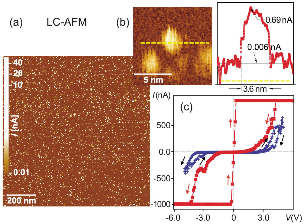
Figure 1: (a) Conductivity map (1 µm × 1 µm) of a 10 nm thick STO thin film recorded by LC- AFM under vacuum conditions; (b) Nanoscale conductivity map (10 nm × 10 nm) and linescan performed along the dotted line; (c) I-V- characteristics of 2 conducting spots with different current load.
We selected single spots on the surface and measured the current-voltage (I-V) curves by applying a DC voltage to the tip. Figure 1c shows two different kinds of I-V curves measured on single-addressed spots in a voltage-driven mode with different current load. Both types of curves show a hysteresis but a completely different switching dynamic. The lower (blue) curve, recorded with a maximum current of 600 nA switches between two branches with a similar non-linear I-V branch, resulting in a maximum ratio between the resitivities in high-conducting (on)- and low-conducting (off)-state (Ron/Roff) of 6. In contrast to it, the upper (red) curve in Figure 1c recorded with a current compliance of 1 µA, depicts switching between a linear on-state branch and a non-linear off-state branch. For this type of switching, a Ron/Roff of several orders of magnitude is obtained. The observed I-V curves can be well explained by regarding the conducting filaments as channels for easy diffusion for oxygen vacancies and location of a current-driven redox-process which induces a local metal-to-insulator transition [5].
Within this model, the different switching curves shown in Figure 1c can be attributed to different levels of reduction within the filaments. Only in the case where the amount of charge connected with the applied voltage is sufficient to completely reduce the filament, the on-state may be metallic (red curve). If the flowing charge is insufficient, parts of the filament remain semiconducting after reduction and cause a non-linear on-state branch in the I-V curve (blue curve).
In order to analyze the distribution of switching events on µm-scale areas and to simulate a macroscopic electrode, we recorded LC-AFM scans after polarizing the surface with a voltage bias of different amplitude and sign. Figure 2a shows a LC-AFM scan which has been switched to the on- and off-state, respectively, on different scan areas. The density of filaments in these scans is so high, that the single filaments can not be resolved and the areas seem to be switched completely.
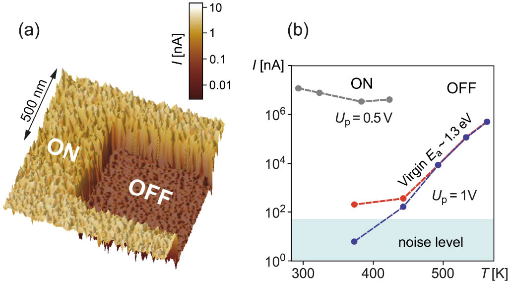
Figure 2: (a) LC-AFM scan of a 10 nm STO thin film; The whole area is scanned with −6 V and subsequently the inner area is scanned with +6 V; B: Temperature dependence of the on-state (grey) and off-state current, determined from LC-AFM current histograms, with (blue) and without (red) noise subtraction (read-out voltage 0.5–1 V; write voltage: 5–8 V; erase voltage: 6 V)
With respect to a deeper understanding of the current transport mechanisms in the different resistive states, in-formation about the temperature dependence of I-V curves of individual filaments would provide a big step forward. Since the thermal drift of the tip prevents experimental ac-cess to this data for a single filament, we instead performed this measurement on large ensembles of filaments by statistically analysing current histograms of LC-AFM scans at different temperatures. The area below the histograms can be identified with the total current across a virtual top electrode with the dimension of the given scan area. Details of this analysis was explained in more detail in reference [3]. Since the filaments are statistically distributed in the sample, the thermal drift of the scan area has insignificant influence on the histograms.
The red curve in Figure 2b shows the temperature dependence of the off-state current determined from the corresponding set of histograms. The noise level depicted in Figure 2b was determined from a histogram recorded with a read-out voltage below the threshold for the observation of conducting spots and can be identified with the experimental noise of the LC-AFM I-V converter. It can be clearly seen, that the off-state current exceeds the noise level for all temperatures above 400 K. The noise-subtracted off-state conductivity (blue curve in Figure 2) which was determined from histograms at the corresponding temperature fits nicely to the Arrhenius law with an activation energy of 1.3eV.
The grey curve in Figure 2b has been determined from current histograms of STO surfaces, polarized with a sufficient negative voltage to completely reduce the filaments. This procedure sets the filaments in the scan area to a linear on-state branch similar to the red I-V curve in Figure 1c. Since the current determined from the corresponding histograms increases with decreasing temperature, the on-state is metallic and its conductivity exceeds the off-state conductivity by 4 orders of magnitude. These results prove that in case of a sufficient current transfer, the filaments are switched between a metallic on-state and a semiconducting off-state.
This scenario is an experimental upper limit for Ron/Roff with respect to a real macroscopic electrode, since scanning with LC-AFM gives a point-to-point galvanic contact on an atomic scale of the free surface and resembles a virtual, almost ideal macroscopic electrode. In real electrodes one has to take into account an imperfect contact with the sample surface or a preparation-induced damage of the interface. Even though many groups report about switching between two semiconducting branches with Ron/Roff in the order of 10 [1], a transition between metallic on-state and semiconducting off-state and a Ron/Roff of several orders of magnitude has already been realized with Pt-top electrodes [6].
In summary, evidence is given that the conduction of thin epitaxial films of STO is filamentary in nature. Depending on the charge transferred to the filaments, different types of hysteretic behaviour are observed. Maximum yield is reached by driving the filaments into the insulator-to-metal transition.
- [1] A. Beck, J. G. Bednorz, Ch. Gerber, C. Rossel and D. Widmer, Appl. Phys. Lett. 77, 139 (2000)
- [2] K. Szot, W. Speier, G. Bihlmayer and R. Waser, Nature Materials 5, 312 (2006)
- [3] K. Szot, Dittmann, W. Speier, and R. Waser, Phys. stat. sol. (RRL) 1, 2 (2007)
- [4] S. H. Oh and C. G. Park, J. Appl. Phys. 95, 4691 (2004)
- [5] K. Szot, W. Speier, W. Eberhardt, Appl. Phys. Lett. 60, 1190 (1992)
- [6] K. Jung, H. Seo, N. Kim, Y. Kim, H. Im, J.-W. Park, M. K. Yang and J.-K. Lee, J. Korean Phys. Soc. 49, 1071 (2006)
K. Szot, R. Dittmann, W. Speier, R. Waser
Dislocation Based Resistive Switching in Insulating Perovskites – An Opportunity for Nanoscale Non-Volatile Memories?
Electrically controlled resistive switching effects have been reported for a broad variety of binary and multinary oxides in recent years. In particular, titanates, zirconates, and manganites have been in the focus of the studies. In many cases, the mechanism of the switching and the geometrical extension of the phenomenon (filaments vs. bulk) are still under discussion. In this work, we present evidence for a redox-based switching mechanism and we indicate a potential route towards highly scalable non-volatile memories based on this switching effect.
Resistive switching effects have been reported for a broad variety of binary and multinary oxides in recent years. In particular, zirconates [1], titanates, niobiates [2], and manganites have been in the focus of the studies. In many cases, the mechanism of the switching and the geometrical extension of the phenomenon (filaments vs. bulk) are still under discussion. In this work, we present evidence for a redox-based switching mechanism and we indicate a potential route towards highly scalable non-volatile memories based on this switching effect.
The challenge our work is to utilize resistive switching mechanism with the aim to construct active electronic elements on a real nanoscale level, here by reversibly switching the electrical properties of individual dislocations by electrical stimuli. We demonstrate that standard undoped SrTiO3 single crystals, utilized as a model system, exhibit a switching behavior along filaments based on dislocations, mediated by oxygen transport. For this, we employed a three-step procedure: the crystals were, at first, annealed at elevated temperatures under reducing conditions, then exposed to 200 mbar O2 pressure at room temperature, and finally subjected to an electric field under ultrahigh vacuum (electroformation). This treatment induced in a metal-insulator (SrTiO3)-metal (MIM) system a transition to metallic state [3]. A hysteretic behavior appears after dynamical polarization of the MIM structure at the maximum electroforming currents. The shape of the I/V curve has the typical signature for bi-stable switching known for these types of perovskites. The positive temperature dependence of the resistance of the low- (LRS) and the high-resistance (HRS) state clearly identifies both states to be metallic in character.
The inhomogeneity of the electrical transport becomes directly evident from a simple optical inspection and the conductivity maps as measured by LC-AFM of a planar structure. One can trace the formation of the filaments, emerging from the cathode and propagating towards the anode during the electroformation process. These filaments are well-oriented along the <100>-axis of the crystal and show a discrete and granular substructure on the nano-scale. The similarity in lateral distribution of exit points (spots) of conducting nano-filaments with respect to the distribution of etch pits suggests that the electrical transport along dislocations determines the micro- and meso-scopic electrical transport phenomena. Our results suggest that a dedicated contact arrangement is required to handle the filamentary conduction in a practical way by using macroscopic electrodes. At the same time, it emphasizes the need to control the relevant processes on the level of individual dislocations.
With LC-AFM(Figure 1) it is possible to specifically address single dislocations crossing the surface with adequate spatial resolution and use the conducting cantilever as the nano-electrode through galvanic point contact. We succeeded to initiate the local electroformation process for a single dislocation by applying a dc bias to the tip of the cantilever. Such nano-prepared dislocations reveal bi-stable switching behavior between a linear and a non-linear I/V-characteristics. The dynamic range of the electrical resistance covers at least 3 to 4 orders of magnitude at read-out voltages of 0.1 V (Figure 2).
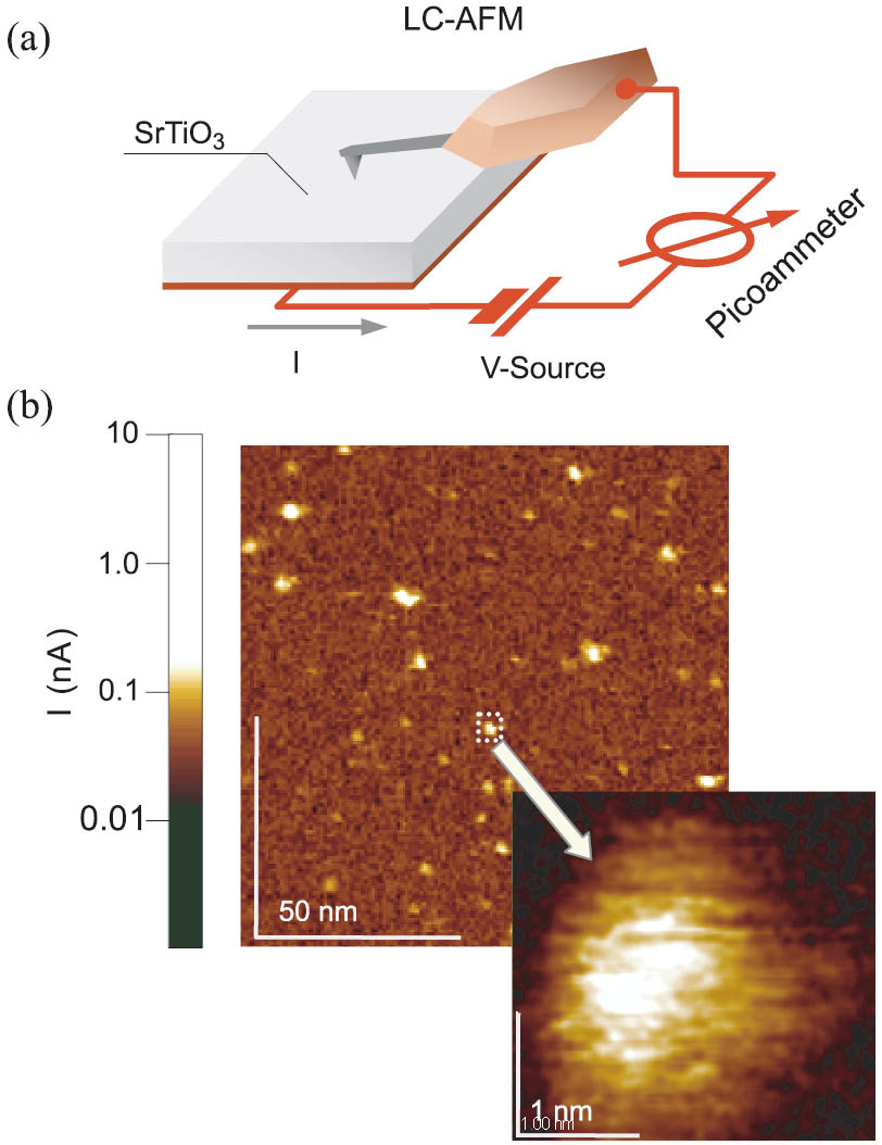
Figure 1: (a) Principle of local conductivity measurements with AFM (LC-AFM). (b) Map of the conductivity at the surface of a SrTiO3 single crystal after short thermal reduction as recorded by the LC-AFM technique.
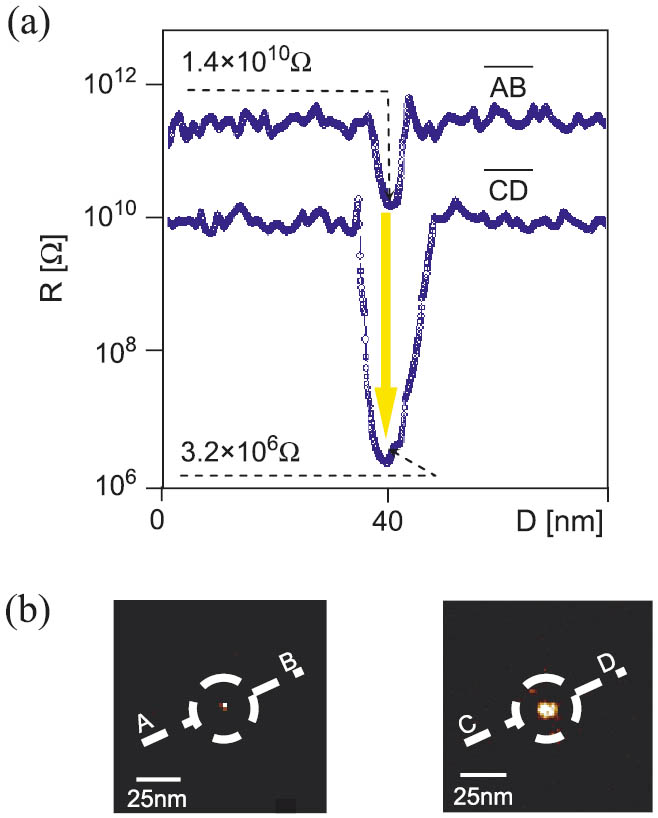
Figure 2: (a) Line scan across a selected spot showing the dynamic range of changes in resistance as a result of the application of a negative tip voltage bias. (b) Maps of conductivity of the selected spot before and after the electroformation process with an increase in diameter at the surface from 5 nm to 10 nm.
In order to develop a microscopic model for the filament, we performed first-principles calculations of extended, linear defects in SrTiO3. Our analyse of electronic structure for extended defects with TiO enrichment establish that already subtle changes in O-content are sufficient to modulate the electronic properties and provide the necessary self-doping capability with a reversible transition between non-metallic and metallic behaviour.
We propose a model for the resistive switching in SrTiO3 based on the modulation of the electrical properties through electrical stimuli in a small segment of an orthogonal network of dislocations [4] (Figure 3). Switching in our case corresponds then to an electrochemical “closing” or “opening” of the single dislocation in the uppermost portion of the network.
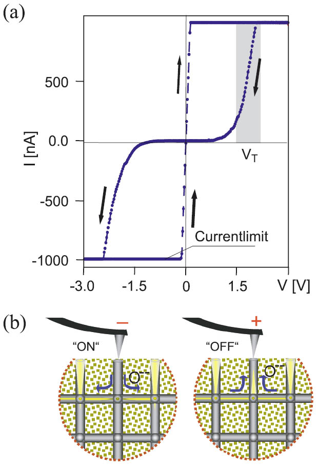
Figure 3: (a) I/V-characteristics of a dislocation crossing the surface of a single crystal with bi-stable switching from a non-metallic to a metallic conductance. (b) Schematic illustration of the electromigration of oxygen in the upper segment of the network causing bi-stable resistance switching with the transition from metallic (ON-state) to non-metallic conductance (OFF-state) at positive and negative tip voltage bias, respectively.
Our results show that the switching behaviour in single-crystalline SrTiO3 is an inherent property of the material and can be easily activated by external stimuli. Due to the availability of dislocation densities up to 1012 cm–2in single crystals and thin film, one can even envisage to approach the Tbit regime, as long as the dislocations can be successfully arranged into registered superstructures.
In summary, evidence is given that the electrical conductance of individual dislocations in a prototype perovskite, SrTiO3, can be switched between a low and a high conducting state by the application of an electrical field. We demonstrate on the basis of ab initio calculations and measurements with a scanning probe microscope SPM that the modulation of the electrical properties is related to the induced change in oxygen stoichiometry and the self-doping capability with a local insulator- metal transition along the core of the dislocations. A model is presented based on a three-dimensional network of such a filamentary structure to analyze the bi-stable resistive switching in the macroscopic metal-insulator-metal (MIM) structure. Our results show that electrically addressing individual dislocations in single crystals as well as epitaxial thin films provides a dynamic range for switching between low and high conducting states which covers several orders of magnitude in resistance and can be of technological interest for the application in Tbit non-volatile memory devices.
- [1] A. Beck, J. G. Bednorz, Ch. Gerber, C. Rossel, D. Widmer, Appl. Phys. Lett.77, 139-141 (2000)
- [2] K. Szot, W. Speier, R. Carius, U. Zastrow, Beyer, Phys. Rev. Lett. 88, 75508(4) (2002)
- [3] K. Szot, W. Speier, W. Eberhardt, Appl. Phys. Lett. 60, 1190–1192 (1992)
- [4] K. Szot, W. Speier, G. Bihlmayer, R. Waser, Nature Materials (in press 2006)
K. Szot, W. Speier, G. Bihlmayer, R. Waser
Co-Existence of Bipolar and Unipolar Resistive Switching in a Pt/TiO2/Pt Thin Film Stack
Bipolar and unipolar resistive switching (BRS and URS) behavior of Pt/TiO2 (27 nm thick)/Pt thin film stacks were investigated. One of both, BRS or URS, could be observed depending on the current compliance during the electroforming process. With a lower current compliance (< 0.1 mA) during electroforming asymmetric current-voltage (I-V) curves showing the BRS were observed in the voltage range −1.6 V to +1.1 V, while with a higher current compliance (1 to 10 mA) the URS behavior was observed. Furthermore, the permanent transition from BRS to URS was investigated by applying the voltage with a higher current compliance (∼3 mA).
Resistive switching behavior of transition metal oxide (TMO) materials is a very attractive subject of scientific and technical research. TMOs, including TiO2 and NiO, show bistable resistive switching behavior, i.e. reversible switching between a high resistance state (HRS) and a low resistance state (LRS) achieved by the applied voltage [1, 2]. This resistive switching is classified into unipolar resistive switching (URS) because the switching behavior hardly depends on the polarity of the applied voltage, so that both, the SET switching (HRS→LRS) and the RESET switching (LRS→HRS), occur regardless of the polarity of the applied voltage. The URS of TMOs gives potential for the application in resistive switching random access memory (ReRAM) devices due to the high off/on ratio and the inherent low geometric scaling problem compared to capacitance-based RAMs. However, a quite high current flow, a few tens of mA, is necessary for the RESET switching of the URS. It is therefore very important for the application to search for solutions with reduced RESET current.
Bipolar resistive switching (BRS), showing a dependence of the resistive switching on the polarity of the applied voltage, has been reported in perovskite-type oxides including SrZrO3, Pb(Zrx,Ti1−x)O3, and Pr0.7Ca0.3MnO3 (See Refs. in [3]). An interesting aspect of the BRS is the low RESET switching current of several hundreds of μA or even less.
A 27 nm thick blanket TiO2 thin film was deposited on a platinized Si-wafer at room temperature by reactive sputtering of Ti in an Ar/O2 environment. As top electrodes (TE) circle-shaped Pt spots with a radius of 100 μm were formed on the blanket TiO2 film by dc sputtering using a lift-off process. The resistance of the as-produced Pt/TiO2/Pt stack is in the GΩ range at 1 V showing good insulating properties [4]. Therefore, to induce URS or BRS, electroforming was carried out by applying a positive voltage of about 5 V on the TE with setting a proper current compliance to prevent permanent dielectric breakdown of the as-produced stack. The current compliance during the electroforming decides on the resistive switching mode: a high current compliance (> 1 mA) leads to URS, while a low one (< 0.1 mA) leads to BRS. However, in the current compliance range of 0.1–1 mA it is hard to define a dominant resistive switching mode because both URS and BRS may be activated [3].
The I−V curve of TiO2 undergoing BRS is shown in Figure 1a, measured with a current compliance of 1 mA and electroformed before by applying a positive voltage on the TE. Switching between HRS and LRS can be observed within the current range (−1 mA to +1 mA). By decreasing the applied voltage from a starting voltage of +1.1 V, the current decreases along the path denoted by (A) in the LRS suggesting that the SET switching takes place by applying the starting voltage. Passing the origin point, negative current increases along the path (B). Around −1 V the RESET switching to the HRS starts with a gradual increase of resistance in the I-V curve until the current compliance (1 mA) is reached at about 1.6 V. Increasing the applied voltage to positive values (paths C and D) the SET switching takes place again around 1 V in the path (D). Both HRS and LRS are stable at a read-out voltage of 0.3 V, for which the resistance ratio of HRS to LRS is about 5 as can be seen in Figure 1b. Figure 1a shows that the I-V curve in the LRS is almost symmetric as long as the applied voltage is less than the RESET switching voltage.
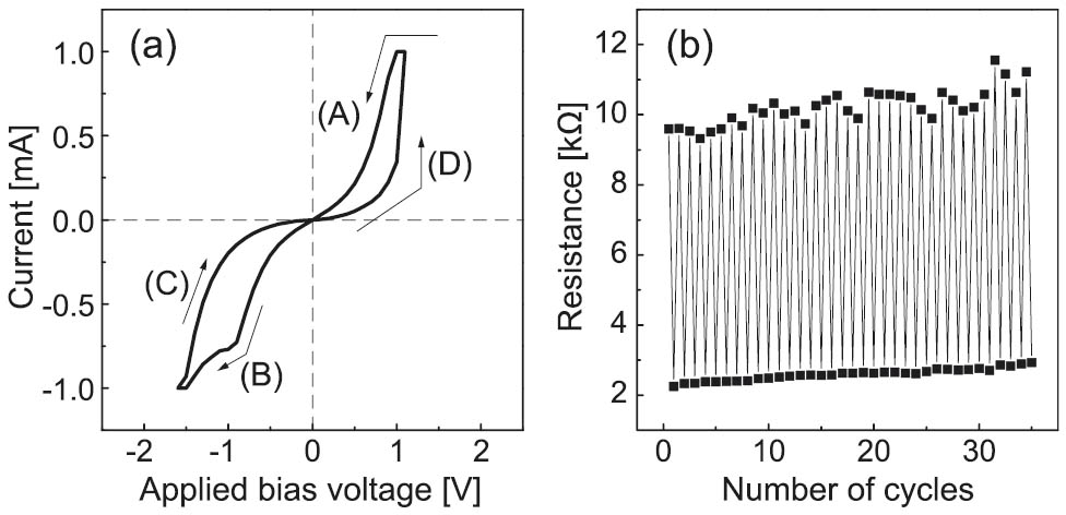
Figure 1: (a) I-V curve of a Pt/TiO2/Pt stack with a current compliance of 1 mA showing asymmetric switching in the BRS mode. (b) The resistances in the HRS and LRS at a read-out voltage of 0.3 V dependent on the number of cycles [3]
Increasing current compliance during BRS gives rise to a transition from the BRS to the URS mode as demonstrated in Figure 2. Several continuous voltage sweeps from +3 V to −3 V (R→L) and back to +3 V (L→R) were applied with a current compliance of 3 mA. Finally, the transition resulted in a linear I-V behavior (5th cycle in Figure 2) corresponding to the LRS of the URS mode. After this transition stable URS behavior is observed in the I-V curves, an example is shown in Figure 3a. The ratio of HRS to LRS is larger than 1000 (see Figure 3b).
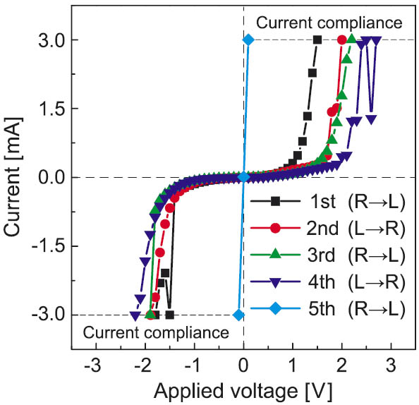
Figure 2: Transition from BRS to URS mode by applying voltage sweeps with a current compliance of 3 mA. R→L and L→R indicate the voltage sweeps from +3 V to −3 V and from −3 V to +3 V, respectively [3].
Comparison of Figure 1b and Figure 3b shows that the resistance values of both resistance states of the BRS mode are in between those of the URS mode, i.e. the HRS and the LRS of the URS mode show higher and lower resistance values than the HRS and the LRS of the BRS mode, respectively. The RESET current of the URS is in the range of 30–50 mA, much higher than that of the BRS (≤ 1 mA). In the shown example, Figure 3a, the current compliance for the SET switching was set to 1 mA, a value lower than the compliance current for the transition from BRS to the URS mode (3 mA) in Figure 2. Therefore, the URS mode is stable as the HRS is very easily switched to the LRS even with a very low current compliance without a reverse transition to be the BRS mode. Another difference of the URS mode of TiO2 is that the RESET switching is accompanied by a steep negative differential resistance phenomenon (see Figure 3a). Comparing Figures 1b and -3b it can also be noted that the resistance values in the LRS with respect to the number of cycles are scattered much less than those of the HRS, especially in the URS mode.
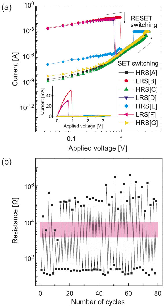
Figure 3: (a) I-V curves in the URS mode in a logarithmic scale; the inset shows same curves in a linear scale. (b) The resistances of HRS and LRS at a read-out voltage of 0.3 V vs. the number of cycles [3]. The pink band indicates the resistance variation in the BRS mode.
In conclusion, it was shown for the first time that BRS and URS modes can be induced in a Pt/TiO2/Pt thin film stack depending on the current compliance value during the necessary electroforming. The BRS mode can be transformed into the URS mode by increasing current compliance during continuous switching cycles, but the reverse transition has not been observed. For the technological application the BRS mode is favored due to its low SET switching current although its resistance ratio of HRS to LRS is much lower than in the URS mode. For a mechanistic modeling more experimental parameters such as temperature, TE area, TiO2 thickness will be investigated together with microstructural observations.
- [1] F. Argall, Solid-State Electronics 11, 535 (1968)
- [2] B. J. Choi, D. S. Jeong, S. K. Kim, C. Rohde, S. Choi, J. H. Oh, H. J. Kim, C. S. Hwang, R. Waser, B. Reichenberg, and S. Tiedke, J. Appl. Phys. 98, 033715 (2005)
- [3] D. S. Jeong, H. Schroeder, and R. Waser, Appl. Phys. Lett., accepted for publication
- [4] D. S. Jeong, H. Schroeder, and R. Waser, Appl. Phys. Lett. 89, 082909 (2006)
D. S. Jeong, H. Schroeder