Sensors and Sensor arrays
Dedicated microsensors such as chemical sensors for specific gases as well as sensor arrays such as artificial skin are required in numerous intelligent systems for a wide variety of applications.
Piezoelectric Microrelay
TASK
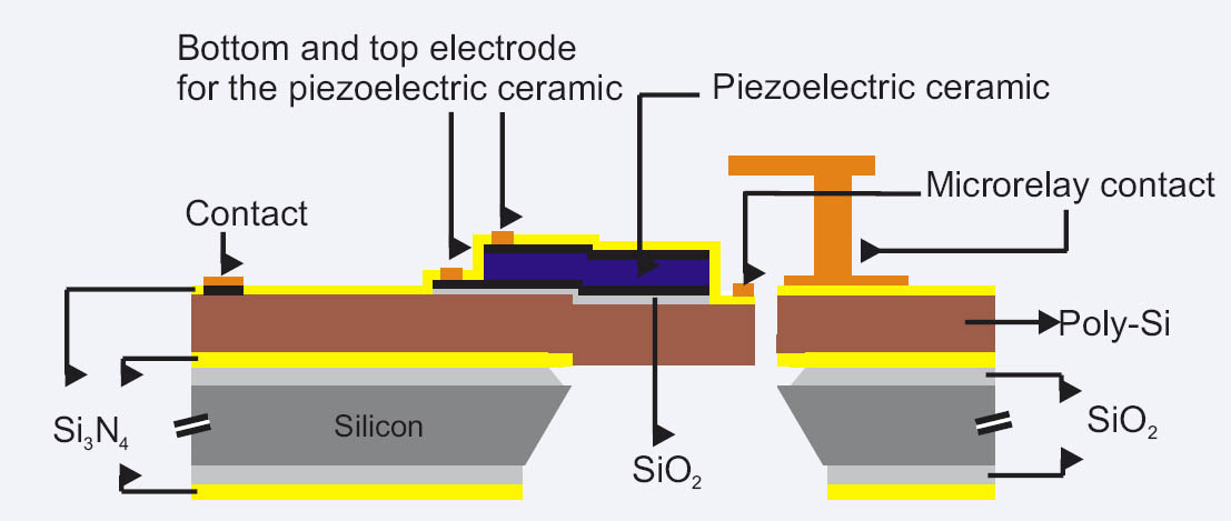
High piezoelectric coupling coefficients of PZT-based material systems can be employed for actuator functions in microelectro-mechanical systems (MEMS) offering displacements and forces which outperform standard solutions. Within this project we developed a micro-relay based on Si bulk micro- machined techniques and integrated ceramic thin films as actuating materials. PZT as the piezoelectric ceramic is prepared by using thin film technologies. Investigations of actuator properties of these films have to be performed.
Next to the high practical importance in respect of galvanic separation for high frequency switching processes the device concept can be used for other micro-machined components as well.
APPROACH
The design of the microrelay has been constituted and all necessary technologies were specified. After the design predetermination of dimensions, energy con-sumption, resistance, and applied tension, the mechan-ical performance is simulated by finite element methods.
The adaptation of ceramic technologies like chemical solution deposition (CSD), reactive ion etching (RIE) and other processes has been followed by the characteri-zation of the thin film layers. XRD, SEM, hysteresis, leakage, fatigue, stress measurements and determination of the piezoelectric coefficient d31 were used to characterize the materials. High attention is also given to the sputtering and patterning process of Pt electrodes to obtain highly <111> oriented and hillock free contacts.
The stress compensation of the complete layer structure is done by an optimized Si3N4 deposition to obtain a planar cantilever.
To demonstrate the feasibility of the technological approach some prototype devices were produced.
RESULTS
First studies of the contact material and the actuating ceramic were performed. The Pt layers are smooth as well as highly <111> oriented. Also a new PZT route was developed, which led to improved electrical properties. RIE processes for both, Pt and PZT, are currently tested and the etched structures are characterized by SEM. The stress values of all layers are measured and primary steps for compensation by an adapted Si3N4 process are examined.
Micro actuator concept with a PZT thin film ceramic as piezo-active material
M. Hoffmann, H. Küppers (IWE I, RWTH Aachen)
Fabrication and characterization of piezoelectric MEMS for integrated switch applications
TASK
Micromachined silicon cantilever beams actuated by the converse piezoelectric effect are of great interest for actuator applications, e.g. micro relays or micro mirrors. For miniaturization and cost saving aspects the combination of silicon bulk micromachining and chemical solution deposition (CSD) technique for the ceramic thin films is very promising.
APPROACH
A significant property for future devices will be the reduction of the required energy. Therefore piezoelectric transducers are most promising for micro switch applications since they exhibit low energy loss, fast response and less area consumption in comparison with the electrostatic, electromagnetic, and electrothermic conversion principle. One desired feature is a high tip deflection to ensure a high off-resistance (open contact) at low applied voltages. The switching distance between the electrodes should be larger than 10 µm.
Before the integration the PZT properties were investigated in detail depending on the Zr to Ti ratio. Figure 1 shows the result of the converse piezoelectric coefficient (d33) measured by double beam laser interferometry. Other results are a relative permittivity of er = 800–1200 and remanent polarization of Pr = 20 − 40 µC/cm2. It turns out that PZT (45/55) is the most suitable material for the integration on silicon.
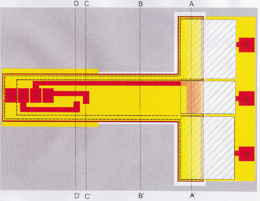
FEM simulations are used to find the ideal dimensions prior the fabrication starts (Figure 2). The model is designed in a way that the most interesting points will be calculated more detailed, e.g. the transition from the silicon to the free standing part. For the realization a combination of surface and bulk silicon micromachining is chosen. Starting with several substrate and masking layers such as polysilicon, SiO2 and Si3N4, a stack of a sputtered Pt bottom electrode, a 350 nm PZT film by CSD and a Pt top electrode is deposited. The structuring of these layers is performed by photo lithography and dry etching techniques. Since mechanical stress compensation is essential a second Si3N4 layer is deposited by PECVD. It also serves as encapsulation. Finally the silicon wafer is etched from the backside by TMAH to free the cantilever. Figure 3 shows a processed 6-inch wafer and detailed picture of a cantilever.
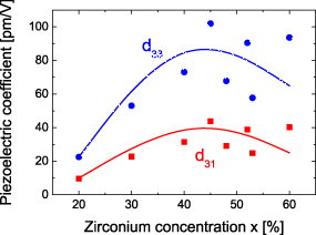
Figure 1: Remanent d33 and calculated d31 of 300 nm thin PZT films with different Zr/Ti ratios.
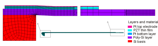
Figure 2: Two dimensional 4-layer FE-model and the simulation grid of a 590 µm long cantilever. Enlargement near the base (b) and of the cantilever tip (c) shows the refinement of the grid model.
RESULTS
Summing-up the results, a PZT thin film actuator for a micro switch application was build. The thin film properties and the performed integration processes correspond to the requirements. As a function of the cantilever length L, a measured tip displacement of d = 3–65 µm and a measured resonance frequency of fR = 0.4–23 kHz were achieved with a PZT layer deposited by CSD as function ceramic (Figure 4). The executed 2D-FEM analyses with a 4-layer model of the actuator confirms these results and matches the measured results much better than analytical calculations.
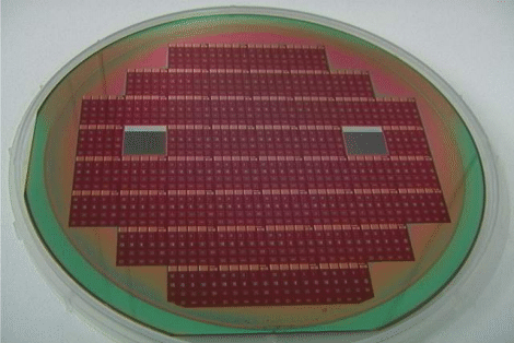
Figure 3: Full processed 6 inch wafer.
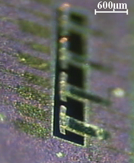
Figure 4: Detailed picture of a freestanding cantilever (avi-video).
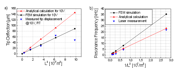
Figure 5: Results of the analytical calculations, the FEM analyses, and the laser interferometry measurements of (a) the tip displacement and (b) the resonance frequency fR.
C. Kuegeler, M. Hoffmann
Pressure Sensor based on Pentacene
TASK
Molecular organic semiconductors are of great interest for low-cost, large-area electronics. Applications like information displays, chemical sensors and electronic paper have been realized. Pentacene organic transistors show performance with mobilities of 1 cm2/Vs and on/off current ratio exceeding 106. This is competitive to amorphous silicon transistors, which are used in LCD displays, but organic semiconductor circuit can be fabricated on flexible substrates and even on paper. In order to develop artificial skin for robotic applications this might be a milestone: Waiting for low-cost pressure sensors based on organic semiconductors.
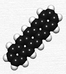
Figure 1: Pentacene molecule
APPROACH
Two different attempts were performed: The examination of the effect of bending pentacene transistors on a flexible substrate and applying pressure by a needle directly to the active semiconductor. In both cases a reversible effect on electrical characteristics has been measured by analyzing the drain-current against the drain-source-voltage.
A SPICE-based model was developed to research into the physical origin of the process. Furthermore a circuit design was proposed and simulated, showing that cross-talk and leakage effects will not affect the functionality of a sensor array.
RESULTS
Both experiments cause a displacement of the switch-on-voltage which is synonymous to the variation of current at a defined voltage. The reason is unknown. The stress/non-stress ratio reaches 1000 %. That effect has been simulated by changing model-parameters “mobility” and “threshold-voltage” only: This suggests that dielectric properties and leakage current remain the same.
These results might be a hint for the extraordinary importance of interlayer-states for reliability of organic semiconductor transistors. Further it shows that there might be an easy low-cost possibility to implement large-area and low-cost artificial skin with accurate and high-resolution pressure sensors.
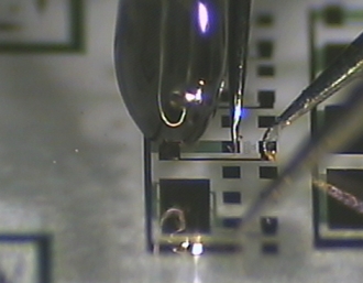
Figure 2: Contacting the bended pentacene transistor.
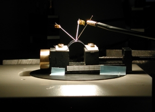
Figure 3: Applying pressure by a needle to an OFET and contacting it.
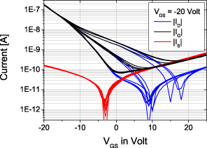
Figure 4: Shifting of the currents.
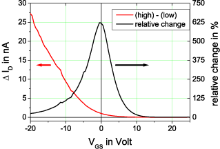
Figure 5: Absolute and relative changing of current.
G. Darlinski
Tunnel Magnetoresistive Elements for Sensor and Memory Applications
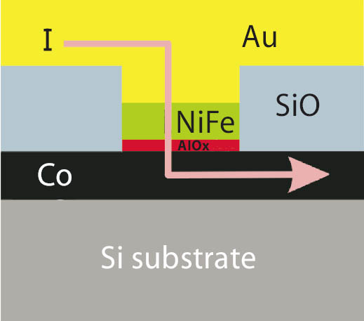
Figure 1: Schematic cross section of a magnetic tunnel junction
TASK
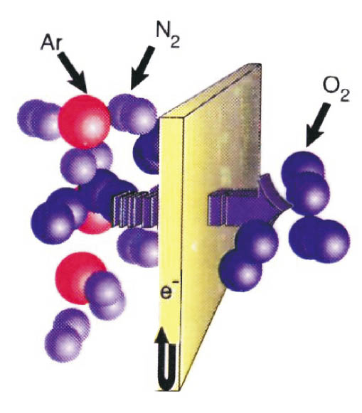
Magnetic tunnel junctions (MTJ) show a large magnetoresistive effect. This resistance change is attractive for large scale integration applications, e.g. sensor devices and the non-volatile magnetic random access memories (MRAM). The tunnel elements are made of ferromagnetic thin films with an insulating interlayer as barrier, usually Al2O3. The preparation and properties of these barriers need to be investigated concerning ΔR/R, temperature and bias dependence, noise, defects, homogeneity and reproducibility, domains, switching characteristics, and fatigue. In order to use these elements in highly integrated memories one needs to fulfill the requirements for the implementation in CMOS technology. In this project, we elaborated a novel method for fabricating tunnel junctions by UV light assisted oxidation.
APPROACH
The tunnel barrier is made of a sputtered Al thin film which is usually oxidized by an oxygen plasma. This results in a very high area resistance (RA). However, in memory appli-cations, where the highly integrated elements are in the sub-µm region, this is undesirable. On the other hand, the RA-product is too small when using thermal oxidation. In our case we followed the idea by Fritsch et al., who described the in-situ oxidation with UV light illumination.
The samples are prepared by sputtering on thermally oxidized Si wafers. The ferromagnetic bottom electrode consists of 19 nm dc-magnetron sputtered Co. The Al (1.3 nm) for the barrier is rf sputtered and then oxidized, assisted by a low-pressure-mercury-lamp (4 W). The process mechanism has been proposed by Cabrera and Mott based on the photo electric effect: during thermal oxi-dation of the Al, electrons tunnel through the forming oxide layer and surface charges are formed. A resulting field pulls positive Al ions through the barrier.
The oxide growth stops as soon as the electric field across the barrier is too small for moving the Al ions. UV light excites further electrons in the metal which pass through the barrier and are trapped at the surface. Increasing the surface charges by the UV-light and, thus, the electric field yields a larger limiting thickness.
The oxygen pressure in the chamber is varied between 1 and 100 mbar. The oxidation time is within a few minutes up to one hour. The top electrode is a sputtered permalloy (Ni81Fe19) layer (18 nm) followed by a wiring layer of Au.
The structure is patterned by optical lithography and ion beam etching.
RESULTS
This preparation method seems to be very suitable for the junction and we receive area resistances in the approp-riate range of 0.1...100 kΩµm2. Processing 3"-wafers with the same oxidation time of 1 h, but different oxygen pressures shows, that the highest TMR-effect is achieved at 10 mbar. It is also seen that all MTJs across the wafer show tunneling I-V-curves as well as ΔR/R > 10%.
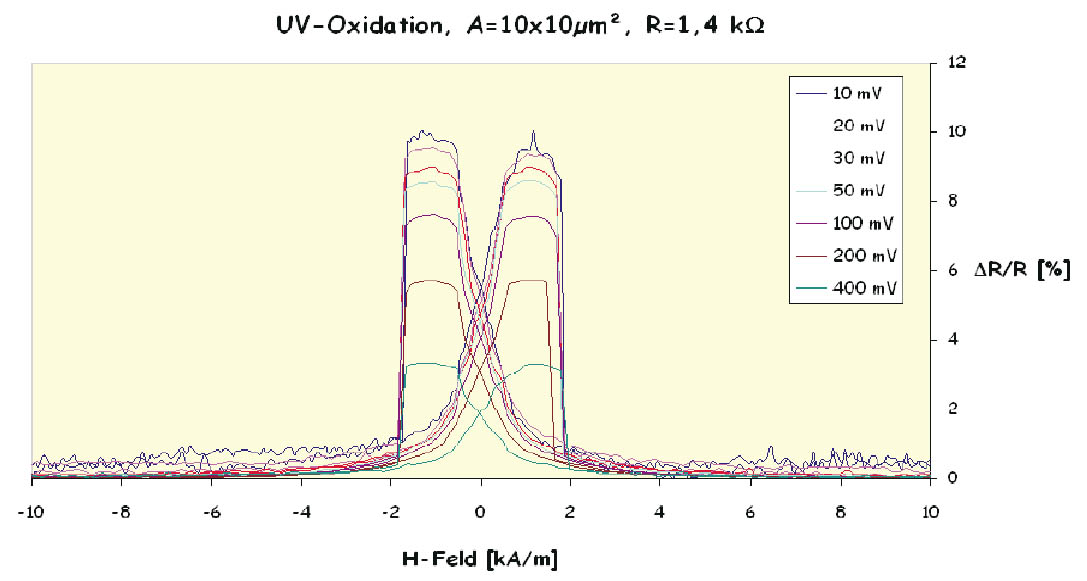
Figure 2: Magnetoresistance plot at room temperature
R. Schmitz, S. Stein, H. H. Kohlstedt
Development of Oxygen-Permeable Ceramic-Membranes for NOx-Sensors High Temperature Proton Conductors
TASK
Continuous improvements in reducing the NOx emissions of combustion engines to meet future legislation standards have led to new catalyst-sys-tems, requiring NOx sensors for optimum performance with respect to On-Board-Diagnose systems (OBD). Within the concept of amperometric sensors the removal of molec-ular oxygen prior to the detection of the NOx level is required. Hence, several mixed ionic-electronic conductors have been investigated with respect to their feasibility as highly selective membranes within a new amperometric sensor system for the detection of NOx in the exhaust gas of lean-burn engines.
APPROACH
Based on extensive calculations concerning the signal generation and the required performance to fulfil the demands for application in vehicles, several promising perovskite-based compositions such as Gd1-xCaxCoO3-d and La1-xSrxCo1-yCuyO3-d as well as composite materials like Gd1-xCaxCoO3-d/Ce1-xGdxO2-d (GCCCGO) have been characterised. With respect to future manufacturing, the determination of surface reactions of the membranes at elevated temperatures has been carried out. In addition, the possibilities to co-fire the membrane materials with Yttria-stabilized zirconia (YSZ) have been evaluated, using thick film technology. YSZ is needed in the sensor for the O2 pumps.
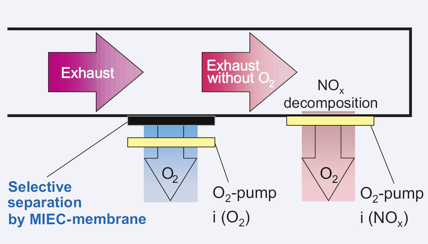
Simplified principle of the NOx-sensor concept
RESULTS
We have shown that Gd1-xCaxCoO3-d hardly promotes the oxidation as well as reduction of the NOx gas species even in the presence of hydrocarbons like C3H6. By means of 18O-isotope exchange experiments the reason for this effect has been determined: an ex-traordinary level of oxygen presence at the surface of the ceramic even at low partial pressures.
Using the well known Hebb-Wagner Point contact method, the ionic conductivity of all membrane materials has been investigated. Taking advantage of the effective medium theory, the optimum component-ratio for the composite ceramic GCCCGO with respect to permeation behavior has been predicted. Accompanied by thermodynamic modeling, we have been able to calculate the stability of all membranes concerning the exposure in sulphur containing atmos-phere. Unfortunately, all MIECs show a tendency to form sul-phates at elevated temper-ature. Nevertheless, using thick film technology, several planar-type structures have been manufactured and have been investigated extensively. Based on experimental as well as modeling data, the overall performance of a system based on GCCCGO has been determined. We have been able to prove the theoretical capabilities of the new measuring concept in syn-thetic gas mixtures. However, poor permeation properties as well as the lack of stability in a sulphur containing environ-ment is still preventing testing in real exhaust gas today.
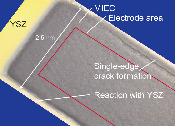
View from the top onto the sensor's surface
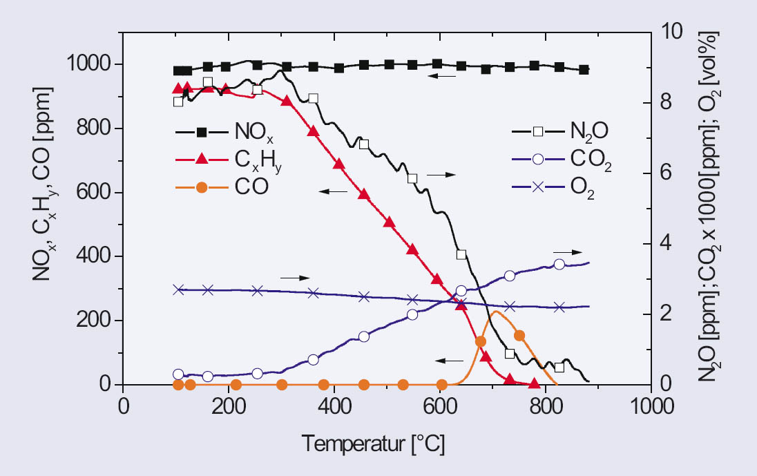
Temperature dependence of the resulting gas concentrations after streaming through a GCCCGO powder plug, demonstrating that NOx is not affected by surface reactions
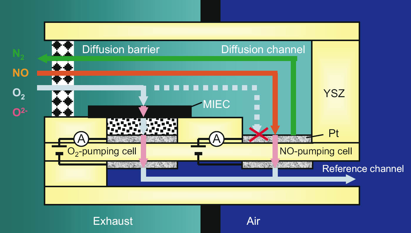
Detailed illustration of the sensor, showing the O2- and NOx-pumping cell
T. Schulte (Bosch GmbH)