Logic devices and nanoarchitecture
Alternative architectures such as programmable cross-bar array and unconventional devices such as all-oxide field effect transistors pave the way to more energy efficient information processing and additional functionalities incorporated into chips.
Sequential Logic Operations in Passive Crossbar Arrays
Passive crossbar memory arrays are the simplest conceivable matrices consisting only of bit and word lines and a storing element, i.e. resistive switch [1], at each junction, resulting in a minimum feature size of 4F2 [2]. Because of the simple structure, crossbar arrays are easy to fabricate and are excellently applicable for 3D integration [3]. Besides array functionality, logic operations are feasible too [4]. In advantageous approach, two anti-serially connected bipolar resistive switches, complementary resistive switches (CRS), are incorporate at each cross-point junction [5], and allowing memory-in-logic functionality [6].
BRS and CRS specification
In Fig 1a, the specifications for bipolar restive switches (BRS) and complementary resistive switches (CRS) are depicted. Both devices offer two terminals, labeled with T1 and T2, respectively. The logic variables p and q, either “0” (low potential) or “1” (high potential) are applied to these terminals. In each case there are two states, Z = “1” (cylinder) and Z = “0” (cube). In Fig. 1b an exemplary I-V characteristic of a BRS cell is depicted. For a positive SET voltage the device switches to state Z = “1”, i.e., the low resistive state (LRS), while for a negative RESET voltage the device switches to Z = “0”, i.e., the high resistive state (HRS). Fig. 1c shows an exemplary I-V characteristics of a CRS cell. Here, Z = “1” corresponds to HRS/LRS and Z = “0” corresponds to LRS/HRS.
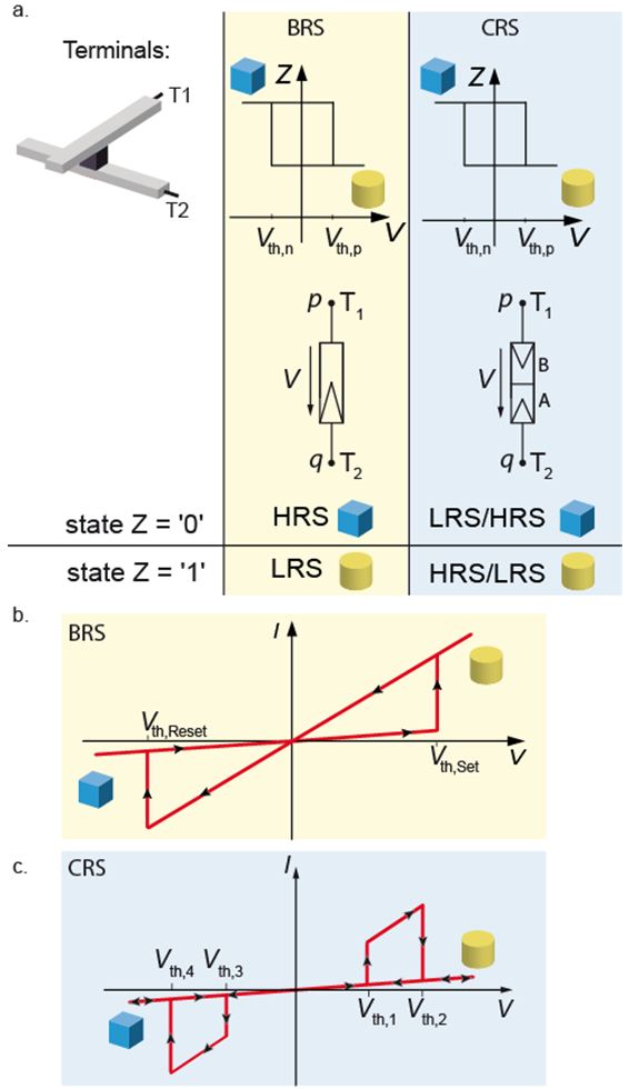
Figure 1: BRS and CRS specifications.
Readout procedure
In Fig. 2a, the read operation of a BRS cell using a level read scheme is shown. A small read voltage is applied to the cell, and the corresponding read current is detected. A high current (state LRS) is assigned to logical “1” output, while a low current (state HRS) is assigned to a logical “0” output. (b) Read operation of a CRS cell using a spike read scheme. Here, a read voltage pulse which is equivalent to a positive write pulse is applied. Therefore, only if the CRS cell is in state LRS/HRS (cube) the cell switches and a current spike occurs. The occurrence of a current spike is assigned to a logical “0” output, and the absence of a current spike is assigned to a logical “1” output. Due to destructive read-out, a write back step is required.
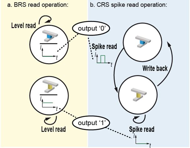
Figure 2: Read operation of a BRS and CRS device.
BRS and CRS logic operation
The basic logic operation of a BRS cell (Fig. 3a) and the logic operation of a CRS cell (Fig. 3b) can be understood from a finite state machine representation. The operations are completely identical for both devices. Variable p is applied at terminal T1 and variable q is applied at terminal T2. When starting from state Z = “0” the negation of the implication function (p NIMP q) is realized, while when starting from state Z = “1” the reverse implication (p RIMP q) is conducted. In Fig. 3c the corresponding logical tables are depicted.
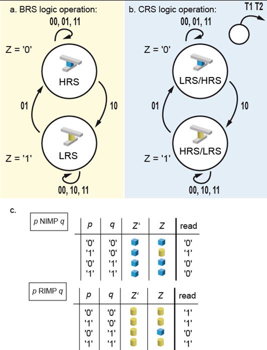
Figure 3: Finite state machine representation of BRS and CRS devices, realizing NIMP or RIMP operation.
However, if the previous state Z' is not known the actual state is defined by a more general equation (see Fig. 4). Regardless of the previous state Z', the cell switches to state Z = “1” if T1 = “1” and T2 = “0” are applied, and to Z = “0” if T1 = “0” and T2 = “1” are applied. For any other input signals, no change of the state variable occurs.
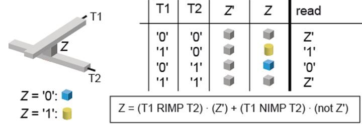
Figure 4: General equation.
Since the logic operation depends on the previous state Z', a stateful logic is possible, and in general, a defined initial state Z' is needed. Thus, the first logic operations needed are FALSE and TRUE, which must always be performed in a first cycle. The logic tables of TRUE and FALSE are depicted in Fig. 5. To expand the logic functionality q and p are not applied simultaneously, but sequentially. Hence, the logic operation is provided by a two or three cycle process. With equation from Fig. 4 and either TRUE or FALSE in the first cycle, the implication based operations can be implemented (Fig. 5).
Note that with TRUE (Z' = 1) the operation for the next cycle is set to RIMP, while with FALSE (Z' = 0) the operation for the next cycle is set to NIMP.
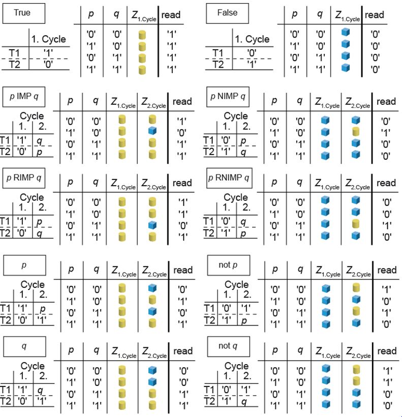
Figure 5: Logic tables for one and two cycle functions.
With a third cycle (Fig. 6), OR, NAND, NOR and AND can be realized, too:
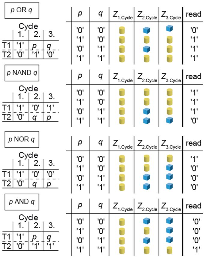
Figure 6: Logic tables for three cycle functions.
Two functions cannot be realized with a single complementary resistive switch or bipolar resistive switch: XOR and XNOR. If these functions are needed, two devices must be connected via a wired AND (“&”).
Note that XNOR and XOR are not required to obtain a functionally complete set of Boolean operators, and it is reasonable to be restricted to 14 of 16 functions for the following reasons:
• only a single device is required for each operation
• the result is inherently stored to memory (state Z)
• each cell in a crossbar array can be either used for logic or memory operation
As stated earlier, this systematic approach is valid for both complementary resistive switches and bipolar resistive switches either, but, since no low-ohmic state is present in CRS cells in any step (apart from the reading process), CRS cells are more favorable for crossbar array implementation.
Conclusion
Using the approach presented here, 14 out of 16 Boolean logic functions can be realized by both, CRS and BRS cells, in at most three cycles and the logic result is directly stored to the memory. For the two remaining logic functions two devices are required. A universal memory, allowing for logic operations in the memory itself, becomes feasible by this approach.
- [1] R. Waser, R. Dittmann, G. Staikov, and K. Szot, “Redox-Based Resistive Switching Memories - Nanoionic Mechanisms, Prospects, and Challenges,” Adv. Mater., vol. 21, pp. 2632-2663, 2009.
- [2] ITRS, “The International Technology Roadmap for Semiconductors - ITRS 2009 Edition”, 2009.
- [3] C. Kügeler, M. Meier, R. Rosezin, S. Gilles, and R. Waser, “High density 3D memory architecture based on the resistive switching effect”, Solid State Electron., vol. 53, pp. 1287-1292, 2009.
- [4] J. Borghetti, G. S. Snider, P. J. Kuekes, J. J. Yang, D. R. Stewart, and R. S. Williams, “‘Memristive’ switches enable 'stateful' logic operations via material implication”, Nature, vol. 464, pp. 873-876, 2010.
- [5] E. Linn, R. Rosezin, C. Kügeler, and R. Waser, “Complementary Resistive Switches for Passive Nanocrossbar Memories”, Nat. Mater., vol. 9, pp. 403-406, 2010.
- [6] E. Linn, R. Rosezin, S. Tappertzhofen, U. Böttger, and R. Waser, “Beyond von Neumann-logic operations in passive crossbar arrays alongside memory operations”, Nanotechnology, vol. 23, pp. 305205/1-6, 2012.
E. Linn, R. Rosezin, S. Tappertzhofen, U. Böttger, and R. Waser
Evaluation of Nano-Crossbar Arrays with TiO2 Resistive Switching Layers for FPGA-Type Logic
The persistent increase of memory integration density expressed by Moore’s law illustrates the demand for ever smaller structures: Nano-crossbar arrays are therefore widely investigated [1]. Nonvolatile and resistively switching materials with two stable states such as TiO2 are integrated as two terminal memory devices to efficiently create a RRAM bit pattern [2, 3].
Figure 1 illustrates how these cells are easily integrated into crossbar arrays where the simple design reduces the cell size per bit to 4 F2 combined with a relative ease of alignment. The switching material covers the whole chip area and every junction at a cross point is an addressable cell of a RRAM. Since the array consists of passive elements, additional active external circuitry is required for the operation. Figure 2 shows the hybrid of an array in combination with CMOS circuits to address the cells, set and reset their state and read the stored information [4, 5].
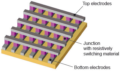
Figure 1: Pattern of a crossbar array. The metallic top and bottom electrode (grey) sandwich the functional layer (pink) of a resistively switching material which is only illustrated at the junctions.
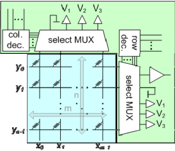
Figure 2: Pattern of a hybrid with a nano-crossbar array memory core (blue) and the CMOS control structures (green).
First, we report on a novel fabrication route to create crossbar arrays in the nanometer range. Structures of Pt electrodes with resistively switching TiO2/Ti layers offer a model system to study the properties of passive crossbar arrays and the specific requirements of these systems concerning external control structures for a CMOS hybrid.
In the second part we present an analytical method that allows the exploration of the complete design space of such crossbar architectures. With this method it is possible to identify the best handling of crossbar structures, to evaluate fundamental limits of crossbar architectures and to generate specifications for the switching material.
Fabrication process
Electron Beam Lithography in combination with a lift-off process is used to fabricate prototype test crossbar structures with a feature size of 100 nm (Figure 3). The lift-off process forms the metal electrodes using a two layer resist on a 1” × 1” Si substrate with a 400 nm thick thermally oxidized SiO2 layer. The bottom resist is a copolymer PMMA/MA with 1 % solid content [AR-P 610.01] and a thickness of 60 nm. The top resist is a PMMA polymer with 1 % solid content and a molecular weight of 950 K [AR-P 610.01] and a thickness of 25 nm. The structure is written with a dose of 200 µC/cm². Finally, the development is performed in AR 600 - 55 for 75 s. As the copolymer is more sensitive to the e-beam than the polymer, this results in a larger expansion of the resist gap of the bottom layer, respectively a staged overhanging resist edge. This is mandatory for well defined metal structures after lift-off and in consequence no additional etching process is required to remove the residual resist in the gap.
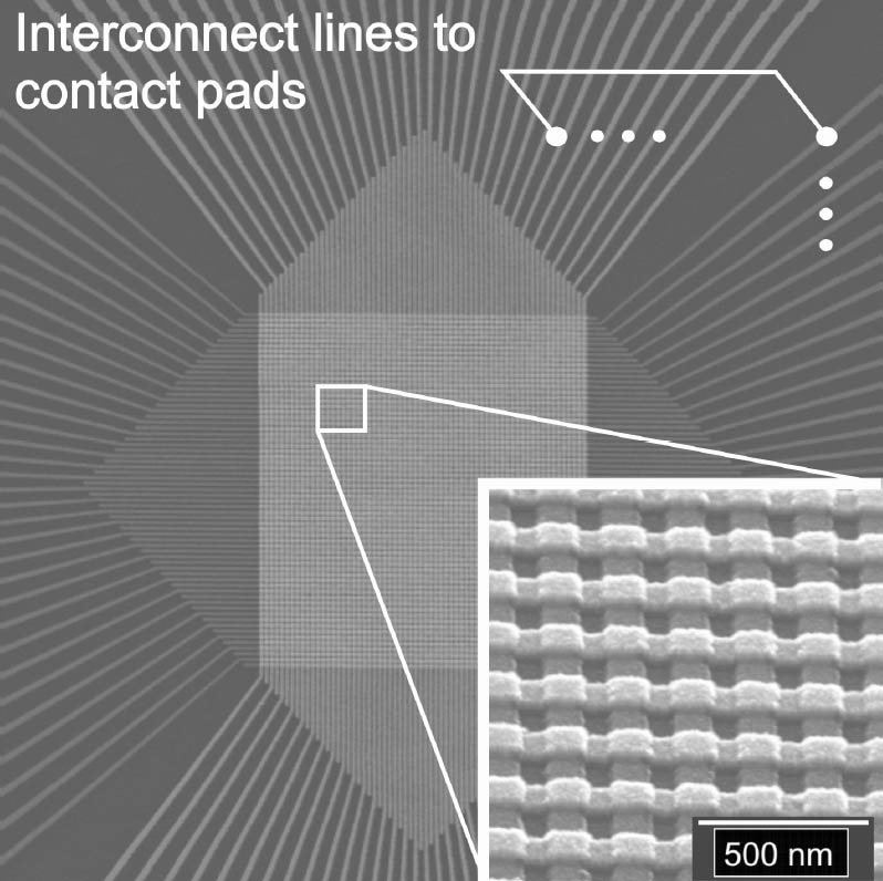
Figure 3: 64 × 64 bit nano-crossbar array with 100 nm half pitch
A combination of 5 nm Ti as adhesion layer with a 20 nm Pt film, which is deposited by electron beam evaporation serves as electrode material. Subsequently a non structured TiO2 layer is deposited via Ti rf-sputtering in an oxygenated atmosphere [6]. Finally, the electron beam lithography and the lift-off process are repeated to create the orthogonally arranged top electrode structures. The fabricated structures comprise single cells (1 × 1 bit), words (1 × n bit) and arrays (n × n bit) with half pitches down to 100 nm and sizes of n = 8, 16, 32 and 64.
Electrical properties
The wire resistance of the bottom electrodes of a 32 × 32 bit array with 100 nm width including the interconnect conductors to the contact pads is 11.8 kΩ ± 500 Ω. The variation arises from different conductor lengths caused by design rules to split up the locally dense array to the large contact pads by interconnect lines. The yield of functional bottom electrodes is above 94 %. The resistance of the top electrode is 14.5 kΩ with a variation of ± 3 kΩ. The yield is larger than 75 %. As the electrodes can be addressed from both sides, the access to each single cell is substantial larger than 71 % which is entirely sufficient for testing. The considered 100 nm electrodes do not show any degradation for currents of 1 mA for 1000 s, considerably more than the current load during operation. With a TiO2 layer as dielectric between the bottom and the top metallization the isolation resistance between neighboring electrodes is larger than 200 Ωm.
Resistive switching of integrated TiO2
Multi crystalline TiO2 shows promising, nonvolatile switching characteristics and is convenient to integrate at room temperature via reactive sputtering. Additionally, the material is temperature stable and compatible with CMOS devices. To get a general understanding of the resistively switching in the integrated 30 nm thick TiO2 layer we characterized a single 100 × 100 nm² cell as shown in Figure 4. The initial state of the cell is high resistive with a resistance of several GΩ and a diode like behavior. A current driven electroforming process with an increasing current (10 nA s−1) initializes the cell into the low resistive ‘ON’ state. Under this condition the cell exhibits a non-linear I(V) characteristic shown in Figure 4. The corresponding R(V) curve is shown in Figure 5.
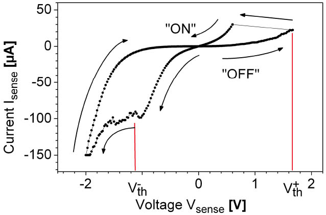
Figure 4: I(V) characteristic of a single 100 × 100 nm² cell via Kelvin measurements
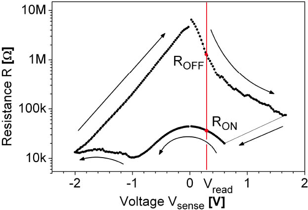
Figure 5: R(V) characteristic corresponding to I(V) in Figure 4
A negative voltage switches the cell to the high resistive, respectively ‘OFF’-state by exceeding a certain threshold value Vth−. This ‘OFF’ state differs for several orders of magnitude from the initial state and is also non-linear. To switch back into the ‘ON’-state, the polarization is changed and a positive threshold Vth+ has to be exceeded. A current limiter prevents the cell from a destructive electrical breakdown at 30 µA which leads to an abrupt jump in the I(V) curve of Figure 4. A nondestructive readout of the cell is performed by voltages within the range from Vth− to Vth+, and the resistance condition is nonvolatile even if no supply voltage is applied. In Figure 5 a read out voltage of 0.3 V exemplifies a resistance of 1.275 MΩ for the ‘OFF’-state and 36.274 kΩ for the ‘ON’-state corresponding to a ratio of 35. The high resistance ratio in combination with a high RON value and the feature of current determined readout instead of charge determination accommodates the demands for a CMOS hybrid.
Analytical Method
We have shown already that with a pure linear IV-characteristic of the material, crossbars can only achieve limited performance [5]. Now we extended this method to allow the analysis of non-linear materials [7].
The basic idea of reading a crossbar is to bring energy to the crossbar and then observe how the energy distributes in the passive crossbar. With this distribution pattern the resistive state at certain positions in the crossbar can be traced back. To make sure that the memory will work, no matter what information is stored in the crossbar, it is essential to identify the worst-case pattern. This is necessary because the performance of the read operation heavily depends on the distribution of ones and zeros stored in the crossbar.
The analytical method used in this work is based on the following steps:
1. Assume the resistance along nano-wires to be Rnw ≪ RON.
2. Group non-accessed junctions according to their position (Rsm, Rsn, Rsmn).
3. Apply homogenous worst case pattern to the junctions in Rsm, Rsn and Rsmn resp.
4. Simplify schematic and solve the Kirchhoff-equations.
5. Identify best parameter-set {Rpd, Rsel, Rpu,s, ROFF/RON} for a maximum ΔVout = Vout,hi − Vout,lo.
Figure 6 shows the best way to address the crossbar if Rj has to be read. After reading Rj, Vout has to be compared with Vout,ref, which can be obtained in a second read operation.
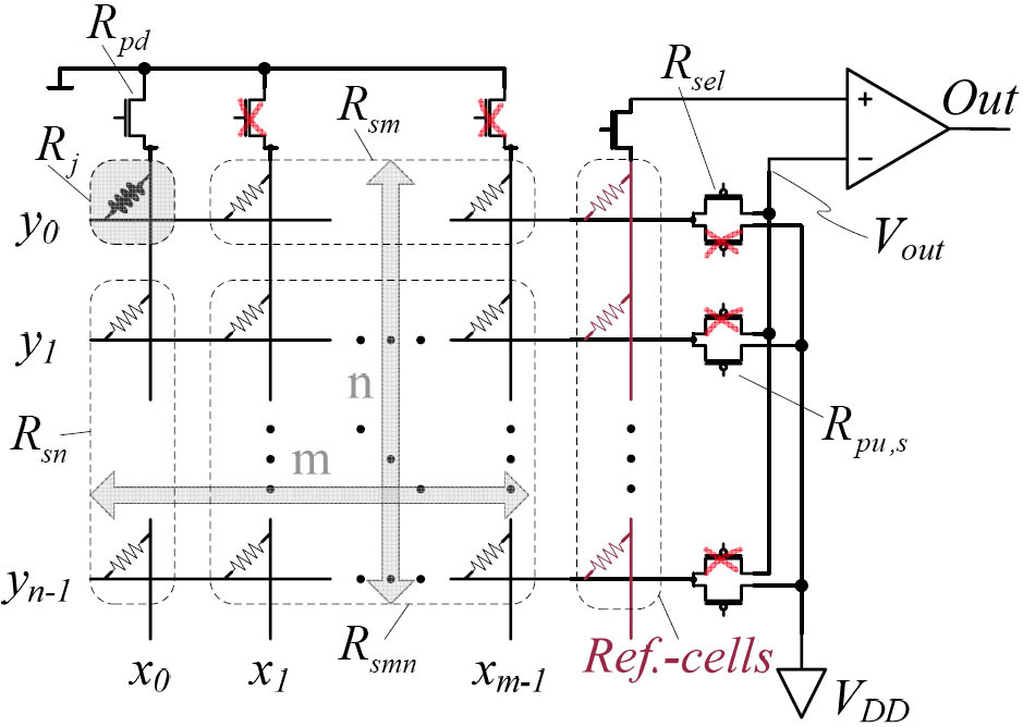
Figure 6: Optimal CMOS setup for read operation.
linear material
Two major statements can be obtained from the analysis for linear materials:
- The RON-resistance in the crossbar has to be at least two to three orders of magnitude larger than the RON-resistance of the CMOS-components.
- At very large ROFF/RON-ratios the maximum voltage swing between reading a high- and a low-resistive state is ΔVout/VDD = O(1/m), where m is the number of wordlines.
If the non-selected nano-wires are clamped to VDD, it is theoretically possible to read unlimited sized crossbars. In practice, the crossbar-size is limited due to economical reasons: If the sense-amplifier that restores the output from the crossbar gets too large, the advantage of small memory-cells is lost. For interesting crossbar-sizes, that enable GBit- and TBit-memory, linear switching behavior leads to an unsatisfactory performance.
non-linear material
The analysis showed that the worst case pattern comprised RON-junctions in the non-accessed cells. A non-linear IV-curve with a reduced voltage over the non-accessed cells can limit this effect. Figure 7 describes the effect on ΔVout: With non-linear devices the load line can be moved towards the optimum (dashed line). This enhances ΔVout. At the same time the operation point of Vout,lo is shifted to higher voltages by the non-linearity in the RON-branch. These two contrary factors result in a global maximum of ΔVout for a certain non-linearity.
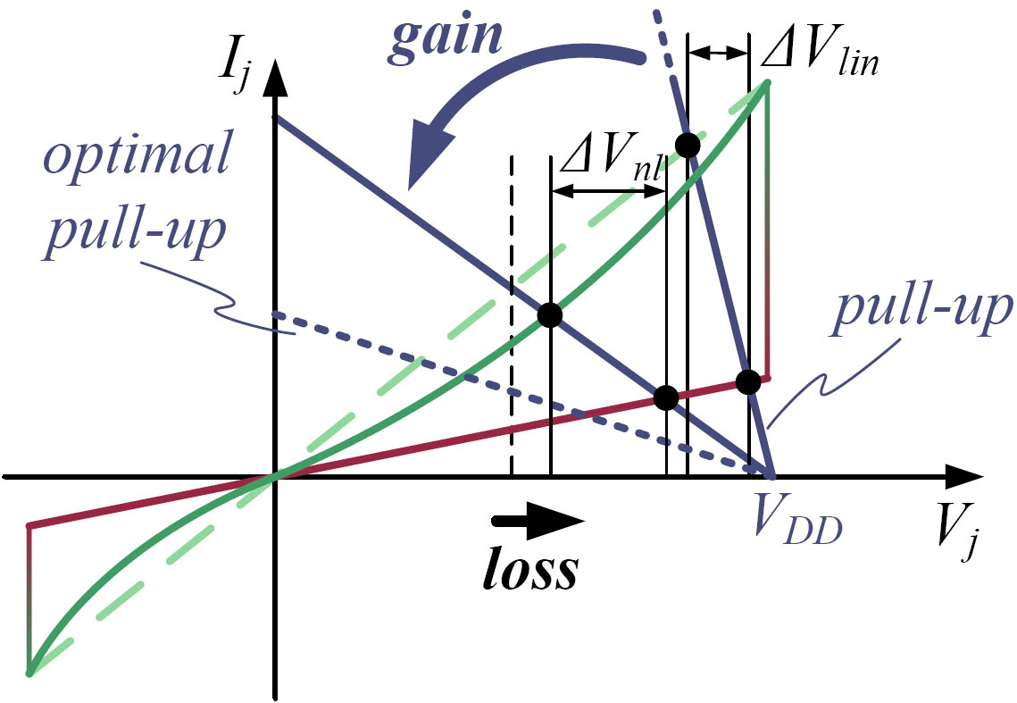
Figure 7: Analysis scheme with non-linear IV-characteristic
Two additional statements can be formed with our analysis for non-linear materials:
- The read-performance increases with a non-linear RON-branch in the IV-characteristic. The performance-gain is limited.
- The read-performance reaches a maximum for a certain non-linearity in the RON-branch. A higher non-linearity decreases the performance.
TiO2 as a resistive material
A variety of switching mechanisms are looked at by material scientists [3]. One promising material is Titanium-Oxide. Figure 8 shows a sketch of the RV-characteristic of a single TiO2-probe. With the RV-characteristic, an ROFF/RON-ratio (here defined at Vj = VDD = 1V, read performance gets better for higher VDD but VDD has to be below Vwrite,hi-lo) and two non-linearity measures ηON = RON, Vj=0V/RON, Vj=VDD and ηOFF respectively can be defined. With our analysis (Figure 9) we can show that TiO2 outperforms any linear material in large crossbar arrays (64 wordlines: TiO2 ≈ 3 %VDD, linear material: maximum 1.6 %VDD). For small arrays (less than 8 wordlines) linear materials with a very large ROFF/RON-ratio yield better results than TiO2.
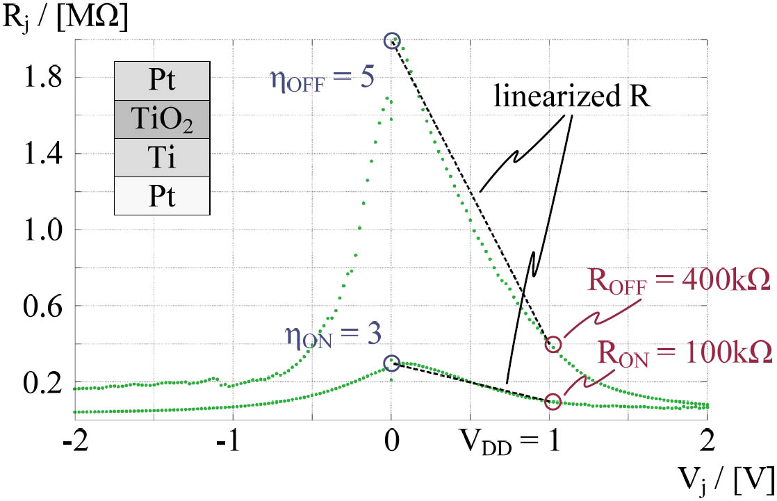
Figure 8: RV-diagramm for a Pt/TiO2/Ti/Pt stack. Layer thickness 30 nm TiO2, 5 nm Ti (top electrode). Cell size: 100 nm × 100 nm.
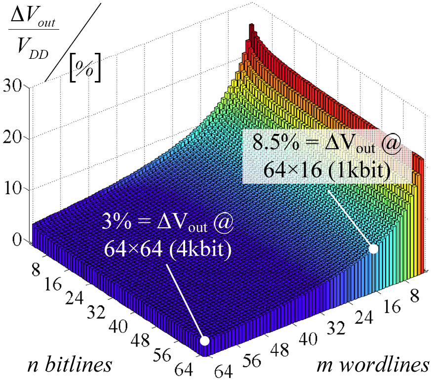
Figure 9: ΔVout vs. crossbar size for TiO2.
Conclusion
We fabricated nano-crossbar arrays by electron beam direct writing and integrated resistively switching TiO2. By downscaling to feature sizes of 100 nm we create addressable patterns with sizes up to 4096 bit and a potential density of 2.5 Gbit/cm². The electrical properties fulfill the demands for the integration and characterization of resistively switching materials.
Our theoretical analysis shows that a non-linear IV-characteristic of the switching material improves the read performance but the impact is limited. At a certain degree the read performance decreases, if the non-linearity of the material increases.
- [1] J. E. Green, J. W. Choi, A. Boukai, Y. Bunimovich, E. Johnston-Halperin, E. DeIonno, Y. Luo, B. A. Sheriff, K. Xu, Y. S. Shin, H.-R. Tseng, J. F. Stoddart, and J. R. Heath, “A 160-kilobit molecular electronic memory patterned at 1011 bits per square centimeter,” Nature, vol. 445, pp. 414-417, 2007.
- [2] A. Beck, J. G. Bednorz, Ch. Gerber, C. Rossel, and D. Widmer, ”Reproducible switching effect in thin oxide films for memory applications,” Appl. Phys. Lett., vol. 7, pp. 139-141, 2001.
- [3] R. Waser, and M. Aono, “Nanoionics-based resistive switching memories,” Nature Materials, vol. 6, pp. 833-840, 2007.
- [4] J. Mustafa, and R. Waser, “A Novel Reference Scheme for Reading Passive Resistive Crossbar Memories,” IEEE Trans. Nanotechn., vol. 5, pp. 687-691, 2006.
- [5] A. Flocke, and T. G. Noll, "Fundamental Analysis of Resistive Nano-Crossbars for the Use in Hybrid Nano/CMOS-Memory," in 33rd European Solid-State Circuits Conference, Munich 2007, pp. 328-331.
- [6] D. S. Jeong, H. Schroeder, and R. Waser, “Impedance spectroscopy of TiO2 thin films showing resistive switching,“ Appl. Phys. Lett., vol. 89, pp. 2909-1-3, 2006.
- [7] A. Flocke, "A General Analysis-Method to determine Fundamental Limits and Requirements for Resistive Nano-Crossbars", in International Solid State Circuits Conference Student Forum San Francisco, 2008.
C. Kügeler, C. Nauenheim, A. Rüdiger, A. Flocke1, T.G. Noll1, R. Waser
1 EECS, RWTH Aachen University
Electronic Properties of Channel Materials for All-Oxide FETs
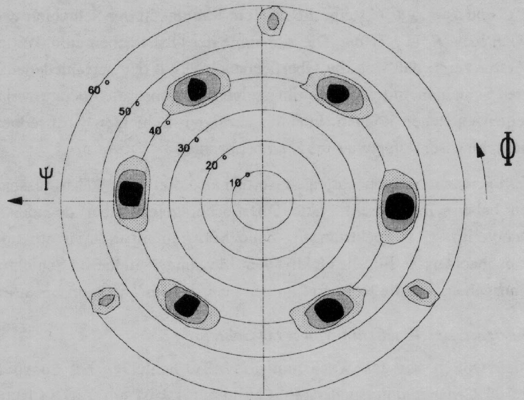
Figure 1: Pole Figure of Sb-doped SnO2 thin film on sapphire
TASK
Field-effect transistors (FETs) with a ferroelectric gate insulator are of interest because of their memory function which can be operated by non-destructive read-out (NDRO). The Philips Research Laboratories in Eindhoven (Natlab) have designed and realized an all-oxide FET on an optically transparent substrate for potential applications in, e. g., displays or projectors. Our task in this joint project has been the investigation of the electronic properties of suit-able channel oxides.
APPROACH
Two different electronically conducting oxides, La-doped SrTiO3 and Sb-doped SnO2, have been deposited by PLD (ArF laser, 193 nm, 350 mJ/shot) on (100) MgAl2O4 and (100) SrTiO3 substrates under different oxygen partial pressure conditions as well as on PZT thin films in the oxi-FET device. The characterization has been performed by conductivity measurements based on the van der Pauw method and by Hall measurements between 10 K and 300 K.
RESULTS
For both types of conductive oxide, the data indicate the formation of impurity bands with an effective mobility of the electrons which is determined by grain boundary barriers. Depending on the deposition parameters, the conductivity can be described by the transition between the thermionic emission over a barrier in a non-degenerated semiconductor on the one hand and a ballistic transport across a point contact (at a grain boundary) on the other hand. A quantitative model has been developed which describes this transient situation and also includes the conductivity of the grain interior. An example of a fit of this model to Sb-doped SnO2 data is shown in the Figure below.
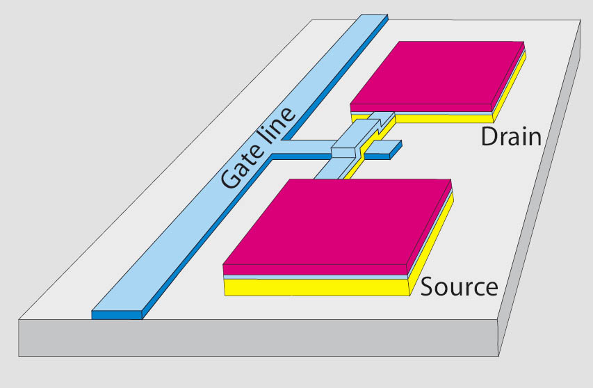
Figure 2: Schematic view of a field-effect transistor (FET) with a ferroelectric gate insulator on an optically transparent substrate
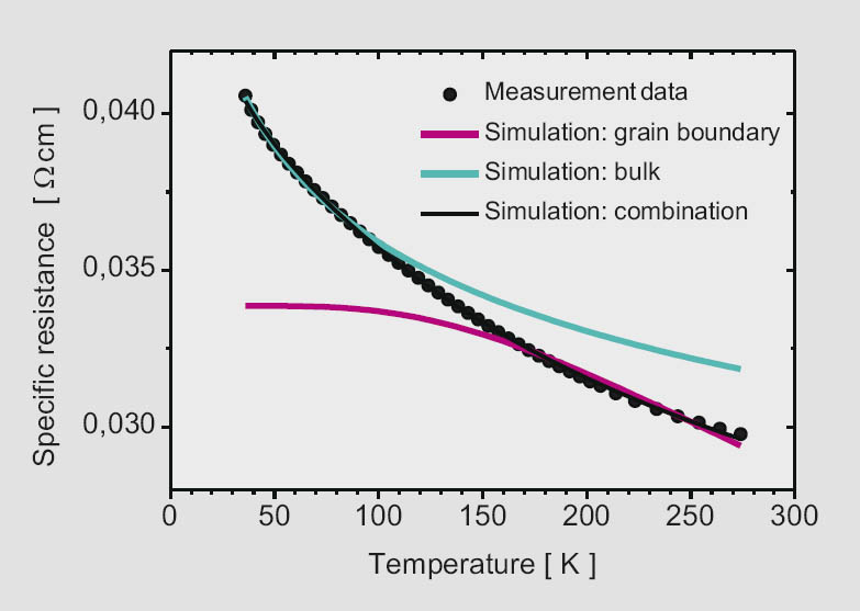
Figure 3: Comparison between measured data and the simulated behaviour based on a quantitative model
K.-O. Grosse-Holz
Superconducting Spintronics: Josephson Junctions with Tailored Ferromagnetic Barrier
Superconductor-insulator-ferromagnet-superconductor Josephson junctions with a thickness step in the metallic ferromagnetic interlayer were fabricated. The step was defined by optical lithography and controlled etching. The step height is on the scale of a few angstroms. Experimentally determined junction parameters indicate a uniform F-layer thickness and the same interface transparencies for etched and non-etched F-layers. This technique could be used to tailor low-Tc Josephson junctions having locally controlled critical current densities, as needed for tunable resonators or magnetic-field driven electronics. It can be extended to other metallic multilayer systems such as magneto-resistance (GMR/TMR) devices where local variation of magnetic properties may enhance their functionality.
The work horse in superconducting electronics is the Josephson junction (JJ). A Josephson junction consists of two weakly coupled superconducting metal bars via a constriction, e.g. made up by a normal (N) metal or a tunnel barrier (I). Various types of JJs are routinely applied in ultra-high sensitive SQUID (Superconducting Quantum Interference Devices) magnetometers or voltage standards. At superconductive/magnetic metal (S/F) interfaces the superconducting order parameter ψ is spatially decaying and oscillating inside the magnet (coherence length ξF1, oscillation length ξF2), whereas for a S/N system ψ is simply decaying inside the metal. By combining the low-Tc Nb/Al technology with magnetic tunnel junctions new functionalities are predicted. In this framework so called 0−π Josephson junctions were recent focus of research activities [1].
The supercurrent through an SNS junction is given by I = Ic sin(φ), where φ = ψ1 − ψ2 is the phase difference of the superconducting electrode wave functions and Ic > 0 the maximum supercurrent through the junction. These junctions are so-called 0 JJs. In an SFS stack with ferromagnetic layer thickness dF ∝ ξF2/2, the amplitude of order parameter ψ vanishes at the center of the F-layer and the order parameter has the opposite sign at the adjacent superconducting electrode. This state is described by a phase shift of π and these junctions are so-called π JJs. SFS or SIFS-type π JJs have a negative critical current, hence the Josephson relation can be rewritten: I = −Ic sin(φ) = |Ic| sin(φ + π). For a variety of JJs a non-uniform critical current density jc is desirable, e.g. for tunable superconducting resonators or magnetic-field driven electronic switches similar to SQUIDs. Our fabrication technology [2] permits the controlled change of only the ferromagnetic interlayer thicknesses d1 and d2 = d1 + ΔdF, i.e. the local jc. The case of non-uniform coupling phase within a single Josephson junction, i.e. one half is a 0 JJ (dF = d1) and the other half is a π JJ (dF = d2) is of particular interest. In such a 0−π junction a spontaneously formed vortex of supercurrent circulating around the 0−π phase boundary with flux |Φ| ≤ ±Φ0/2 inside the JJs may appear [3]. The requirements for SIFS 0−π junctions are challenging. Here we present our technology background for stepped junctions with the focus on small parameter spreads. Our approach represents a considerable step forward to fulfil the extreme requirements on the implementation of conventional or quantum computing devices based on Josephson junctions.
The deposition and patterning of the stepped SIFS junctions was performed by sputtering and a four level photolithographic mask procedure. The F-layer was deposited with a gradient of thickness along y-axis on the S/I stack. The patterning of the desired step-like variation in dF was done after the complete deposition of the SIFS stack. The parts of the JJ that were supposed to have a larger thickness d2 were protected by photoresist, see Figure 1. The step patterning process is depicted in Figure 1a–c. The Nb cap layer was removed by reactive dry etching using SF6 with a high selectivity to the photoresist. A few tenth of nanometer ΔdF of Ni\Cu were Ar ion etched at a very low power and rate to avoid any damaging of the Ni\Cu film under the surface and to keep a good control over the step height. When the F-layer thickness was reduced down to the thickness d1 the etching was stopped and 40 nm of Nb were deposited. The complete etching and subsequent Nb deposition was done in situ. The chip contained stacks with the new F-layer thicknesses d1 (uniformly etched), d2 (non-etched) and with step in the F-layer thickness from d1 to d2. The wedge shaped interlayer (Figure 1e) facilitates the quick fabrication of samples with various F-layer thickness and, at the same time, a low junction to junction deviation.
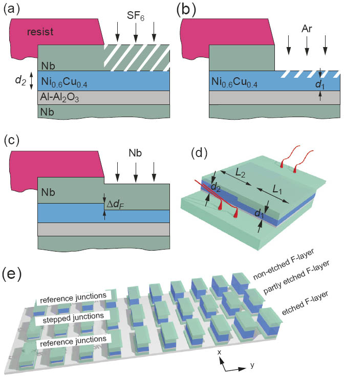
Figure 1: (a) reactive etching of Nb with SF6 down to Ni\Cu layer, (b) ion-etching of Ni\Cu to set 0 coupling, (c) in situ deposition of cap Nb layer. Schematic layouts of stepped JJ based on SFS/SIFS technology (d) and of stepped JJ along with planar reference junctions (e). The F-layer (blue) thickness increases from left to right.
Figure 2 shows IVC and Ic(H) dependences for a non-etched junction (dot) with the F-layer thickness d2 = 5.05 nm and a uniformly etched junction (star) with thickness d1 = d2 − ΔdF = 4.75 nm. Both junctions were 0 coupled. The step height is ΔdF = 0.3 nm. The insets of Figure 2 show the IVCs for small and large ranges of bias current. Besides the difference in Ic, the Ic(H) dependence and the IVCs (right inset) showed no evidence for an inhomogeneous current transport for both samples. The larger Ic, but same resistance R and capacitance C led to a slightly hysteretic IVC of the etched sample. The resistance R is nearly independent from dF as the voltage drop over the tunnel barrier is much larger than the serial resistance of a few nanometer thick metal [4]. A change of capacitance C would require a change of R, as both are determined by the dielectric tunnel barrier. Figure 3 depicts the measured magnetic diffraction pattern Ic(H) of a stepped JJ along with calculated Ic(h) curves. Both junctions halves are 0 coupled. The magnetic field axis h was scaled to fit the first measured minima of Ic(H). Due to the rather steep slope of the jc(dF) curve near the 0 to π crossover jc is very sensitive to d1 and d2. We calculated Ic(h) (dashes) using d1 = d2 − ΔdF = 4.68 nm and d2 = 4.98 nm determined from reference junctions. Then d2 was decreased by 0.04 nm (dots) and finally ΔdF increased by the same thickness, too (dashes-dots). The final calculation has the best agreement with data, although the total interface roughness (rms) of the multilayers should exceed 0.04 nm by far. The measurement and simulation in Figure 3 show the good estimation and control of F-layer thicknesses.
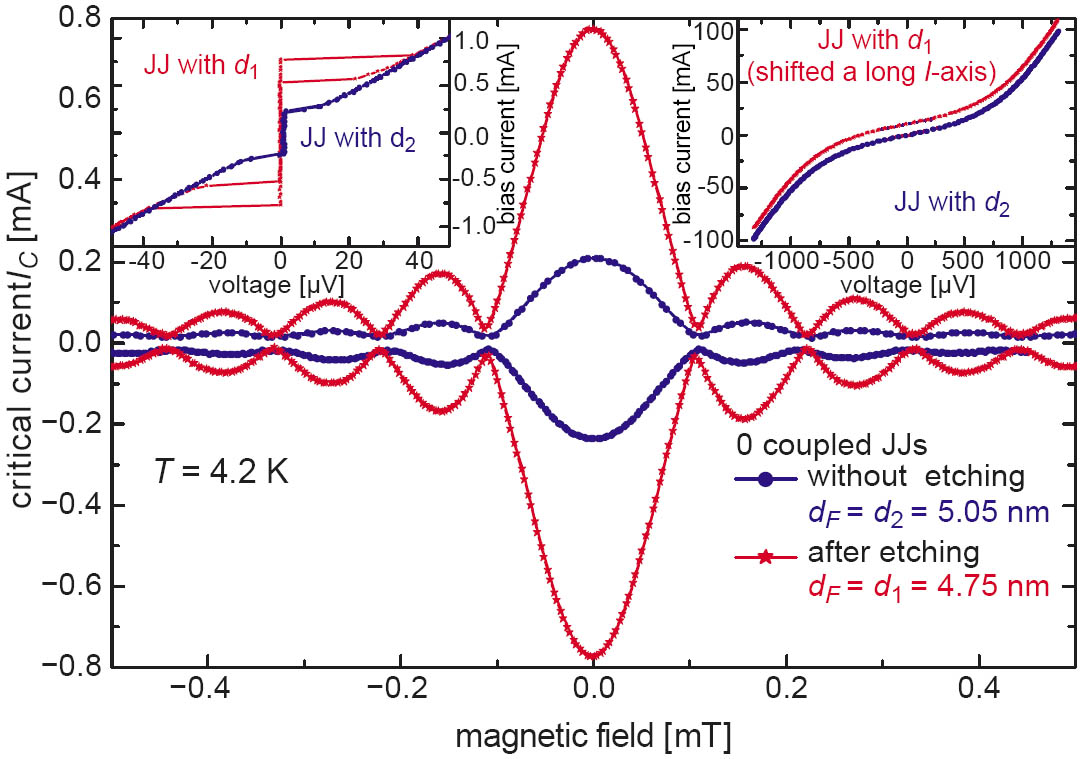
Figure 2: Ic(H) of etched (star) and non-etched (dots) JJs. The insets show IVCs for small and large bias current ranges in zero magnetic field. Both JJs are in the short JJ limit.
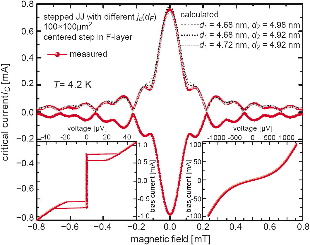
Figure 3: Ic(H) of a stepped 0−0 JJs (square shaped with 100 πm junction length) with d1 = 4.68 nm and d2 = 4.98 nm (determined from reference JJs) plus calculated Ic(h).
Josephson junctions with a step in the ferromagnetic layer were fabricated. The etched and non etched SIFS junctions differ only by F-layer thickness. No inhomogeneities can be seen in the current transport characteristics of the etched junctions.
The patterning of stepped JJs allows free lateral placement of well-defined jc’s and/or local coupling regimes within a single junction. The patterning process could be adjusted to all thin film multilayer structure providing that the reactive etching rates of the layer materials differ. JJs with varying jc and planar phase could be used for devices with special shaped Ic(H) pattern or tunable superconducting resonators. The 0−π SIFS JJs with stepped F-layer allow to study the physics of fractional vortices with a good control of the ratio of symmetry between 0 and π parts.
M. W. is supported by DFG (project WE 4359/1-1).
M. Weides, H. Kohlstedt