Conductive Oxygen Diffusion Barrier for High-κ Oxide Materials on Silicon Electrodes
In order to integrate high-κ oxide materials into CMOS capacitor dielectric or to use their superior dielectric property for capacitive stimulation of nerve cells directly on silicon chips it is necessary to prevent the formation of series-connected layers of low-κ materials such as SiO2. We have developed a thin film layer stack with a conducting diffusion barrier, TaSiN, directly on a highly doped p++Si chip used as bottom electrode in a metal/insulator/metal (MIM) thin film capacitor stack. Using (Ba,Sr)TiO3 (BST) as dielectric in this stack the relative effective dielectric constant was up to 450 with leakage currents lower than 10−6 A/cm2 at voltages lower than 2 V, reasonable values for the mentioned applications.
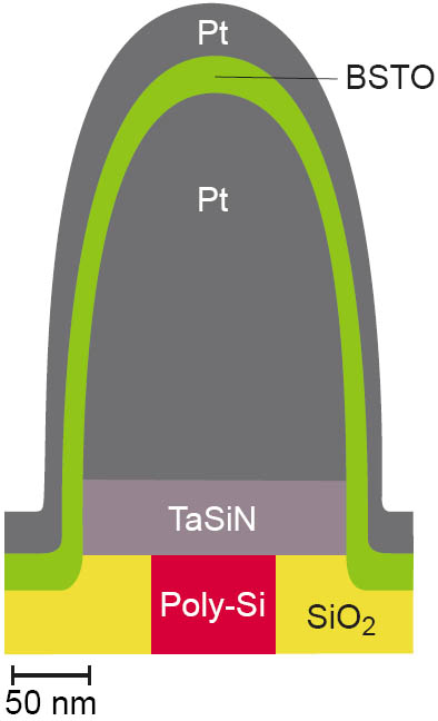
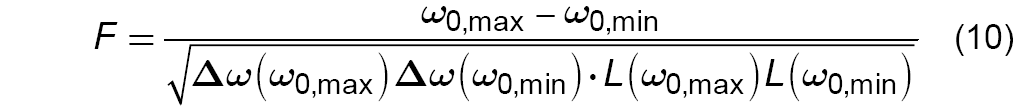
Figure 1: Cross sectional sketch of a prototype of Pt/BST/Pt post capacitor suitable for integration in 1GBit DRAM generation (feature size = 0.2 µm) [2].
For the year 2011 at the latest, the semiconductor industry calls for the integration of high-κ materials (κ > 100) in CMOS based chips, e.g. as capacitor dielectric in stacked DRAM cells, as documented in the International Technology Roadmap for Semiconductors [1] A prototype sample of a post-capacitor is shown in Figure 1 [2]. The via of conducting poly-Si connecting to the CMOS region is separated from used Pt/(Ba,Sr)TiO3(BST)/Pt thin film capacitor stack by a conducting diffusion barrier layer, TaSiN, to prevent mainly oxygen transfer from the BST through the Pt grain boundaries to the poly-Si surface and the possible formation of a series-connected low-κ SiO2 layer, which would degrade the benefit of the high-κ BST dielectric. Unfortunately, an insulating TaSi(O,N) layer has formed at parts of the interface Pt/TaSiN. This layer would have a similar unwanted effect as SiO2 if covering the whole interface area. Another possible application for high-κ materials on Si is the capacitive stimulation of nerve cells for investigations of the interaction at electric interfaces between chip based circuits and living cells as sketched in Figure 2a [3]. Up to now TiO2 (medium-κ ≈ 40) or similar HfO2 are used for this purpose as can be seen in Figure 2b [4]. It is also shown that a very thin insulating low-κ SiNx layer is present reducing the effective dielectric constant to less than 40. Therefore, the use of a BST layer with κ of some hundred separated by conducting barrier layers from the Si would improve the capacitance considerably.
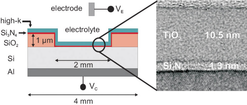
Figure 2: Left: Principle setup for measurements of neuronal activity by capacitive stimulation [3]; Right: TEM cross sectional micrograph of a “state of the art” thin film stack with TiO2 (k ≈ 40) + SiNx (k ≈ 7) as dielectric layers on conductive Si [4].
The main challenge for a good conducting bottom electrode with a barrier layer for the above applications is the thermal stability at the necessary high temperature for depositions or anneals of the dielectric layer in order to assure a high-κ material. Common obstacles are: a) Unwanted reactions within the layers or between them with formation of a non-conducting, low-κ dielectric layer; b) Changes of the microstructure such as recrystallization of amorphous parts or grain growth of crystalline parts sometimes resulting in unacceptable roughness for the thin films.
An optimized stack structure as bottom electrode for these applications has been developed [5] which is sketched in Figure 3. The base is a wafer of very highly doped and therefore good conducting Si(p++) on which three additional conducting thin films have been deposited by DC-sputtering (Pt, Ir) and RF-sputtering (TaSiN). The usual Si-oxide layer has been removed by etching before the deposition of the Pt film. This intermediate layer is necessary as it was found that a stack p++Si/TaSiN develops an unacceptable high contact resistance when annealed at 500–700 °C in oxygen ambient to simulate the recrystallization anneal for the high-κ oxide dielectric. This suggests the formation of an insulating layer at the p++Si/TaSiN interface. In contrast, the stack p++Si/Pt/TaSiN was found to keep very good conduction properties (that of the dominating thick p++Si wafer) and excellent surface smoothness after anneals up to 700 °C with an rms-value of < 0.7 nm. It should be mentioned that during the anneals at T ≥ 500 °C the intermediate Pt thin film (100 nm) reacted nearly completely with the Si substrate by forming conductive platinum-silicides (PtSi,Pt2Si, Pt3Si) as detected by X-ray diffraction. Immediate deposition of a high-κ dielectric layer (BST) on the stack p++Si/Pt/TaSiN and subsequent anneals at 500–700 °C in oxygen ambient once more resulted in a non-conducting, low-κ layer at the interface, largely reducing the effective dielectric constant. Therefore, another metal protection layer was introduced (Pt or Ir) which terminates the bottom electrode stack, p++Si/Pt/TaSiN/Ir(Pt). Unfortunately, the upper metal layer developed unacceptable roughness and reacted with the TaSiN underlayer, when annealed in oxygen at T ≥ 500 °C. The Ir-layer was used because it properties were tolerable for Tanneal < 600 °C, 50–100 °C higher than for Pt-layers. These facts limited the deposition and annealing temperatures for the high-κ oxide dielectric to about T ≤ 550 °C. Therefore, in the optimized stack structure the Ba0.7Sr0.3TiO3 was deposited at 550 °C by pulsed laser deposition and subsequently annealed at that temperature in oxygen. In order to perform electrical measurements structured Pt top electrodes were deposited by a lift-off lithographic process.
Figure 3: Scheme of Cu/p++Si/Pt/TaSiN/Ir/BST/Pt(top) stack used for a electrical characterization showing different bottom electrode configurations for the capacitor thin film stack [5].
Several different TaSiN compositions were investigated. They were produced by reactive RF-sputtering from two TaSix targets (x = 1, 2.7) with different mixtures of argon and nitrogen as sputter gas, different sputter power and at temperatures between RT and about 500 °C. The optimized barrier was Ta28Si28N44, produced at RT with 200 W sputter power and Ar99N1 sputter-gas, the composition was determined by Rutherford back-scattering experiments.
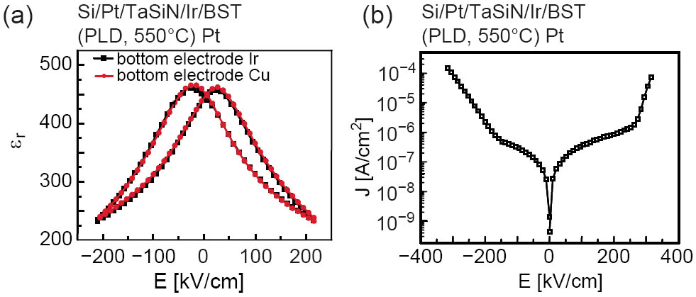
Figure 4: (a) Relative permittivity and (b) Leakage current in a Cu/p++Si/Pt/TaSiN/Ir/BST/Pt(top) capacitor stack after BST deposition at 550 °C with PLD and RTA annealing at the same temperature in oxygen [5].
Electrical data of the stack p++Si/Pt/TaSiN/Ir/BST/Pt(top) are presented in Figures 4a and -b for effective relative dielectric constant κ and leakage current, respectively. The effective κ was measured with two different bottom electrodes, as sketched in Figure 3, the intermediate Ir giving a common MIM capacitor and the bottom of the p++Si wafer metallized with Pt and Cu measuring the whole stack, respectively. The two curves in Figure 4a are nearly perfectly identical showing no considerable influence of the multi-layer electrode stack as desired. The dielectric properties are very reasonable: The peak value of κ ≈ 450 at nearly zero field demonstrates a large advantage for the biological application compared to the used dielectrics. The curve is largely tunable, the slight tendency to a butterfly curve may indicate some ferroelectricity in the thin BST film. The leakage current (Figure 4b) is not completely symmetric expected for the different top and bottom electrode. The absolute current is below 10−6 A/cm2 for fields lower than ±200 kV/cm corresponding to ±2 V, which reasonable for DRAM applications.
- [1] http://www.itrs.net/Links/2006Update/2006UpdateFinal.htm<
- [2] D. E. Kotecki et al., IBM J. Res. Develop. 43, 367 (1999)
- [3] P. Fromherz, Neuroelectronic interfacing: semiconductor chips with ion channels, nerve cells, and brain, Ed. R. Waser, Wiley-VCH, Berlin, 781ff (2003)
- [4] F. Wallrapp, P. Fromherz, J. Appl. Phys. 99, 114103 (2006)
- [5] B. Mesic, Thesis TH Clausthal 2008, to be published
B. Mesic, H. Schroeder
Barium Titanate Zirconate: An Alternative Dielectric Material for Future DRAMs
TASK
Dielectric perovskite thin films of (Ba1-xSrx)TiO3 (short: BST) are widely investigated for inte-grated capacitors and storage node capacitors in future Dynamic Random Access Memory (DRAM) chips. It is known from conventional bulk ceramics that a Sr substitution in BaTiO3 shifts the ferro-electric to paraelectric phase transition towards lower temperatures. Thus, the solid solution Ba0.7Sr0.3TiO3 exhibits a high-K paraelectric behavior at room temperature. The high permittivity value makes BST thin films one of the preferred candidates for DRAM applications, but other decisive factors like low dielectric losses, low leakage currents, and a long life time under dc voltage stress have to be met. In this respect, the dielectric material has still to be improved. Within this project, we present an interesting alternative mate-rial.
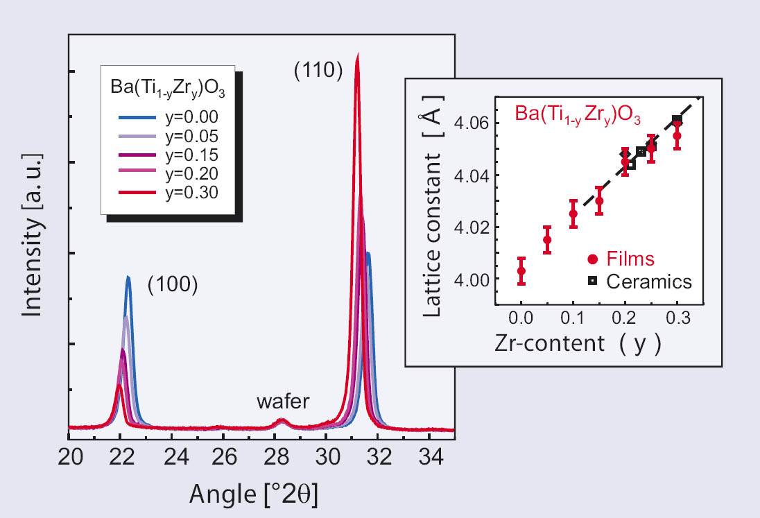
Figure 1: X-ray diffraction patterns and lattice constants of CSD-prepared Ba(Ti1-yZry)O3 thin films deposited on Pt /ZrO2/SiO2/Si-substrates at temperatures of 750°C
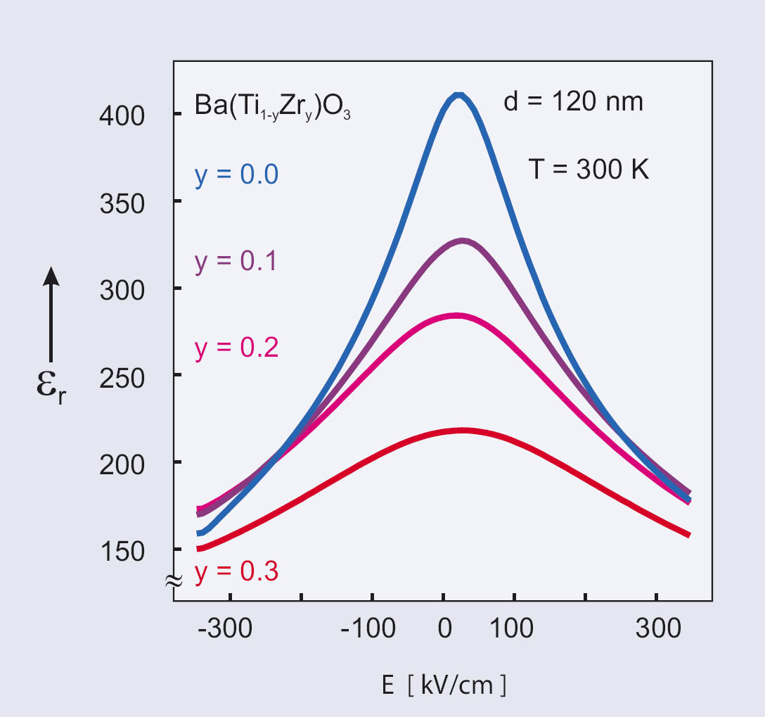
Figure 2: Field dependence of the permittivity (tunability) of 120 nm thick Ba(Ti1-yZry)O3 thin films at T = 300 K and f = 10 kHz; structure: Pt/BTZ/Pt
APPROACH
An alternative BaTiO3 based material which also exhibits a paraelectric behavior at room temperature is the solid solut-ion of barium titanate zirco-nate. Ba(Ti1-yZry)O3 (short: BTZ) is already widely used as dielectric base material in ceramic multilayer capacitors. Investigations on ceramics have shown that in com-parison to alkaline earth titanates the zirconates are more stable with respect to temperature and degradation effects.
Therefore, a comprehensive study on BTZ thin films was performed. Films with up to 30 at% of Zr were grown by a chemical solution deposition method onto Pt coated Si-substrates at temperatures of 750°C. The crystal structure of the films was studied by XRD analysis and the morphology was investigated by SEM and TEM methods. The electrical characterization, which was performed on MIM-structures comprises dielectric analysis and transient impedance analysis with respect to relaxation, leakage, and resistance degradation.
RESULTS
The perovskite phase formation of the polycrystalline thin films was confirmed by XRD analysis for all compositions. The derived lattice constants of the pseudocubically indexed patterns are close to the values reported for bulk ceramics.
The moderate decrease of the permittivity with increasing Zr-content is attributed to the reduction in grain size. For potential DRAM applications, this is partly compensated by a reduction in the dc bias voltage dependence of the permittivity (tunability) for the Zr-rich films.
The capability of maintaining the stored charge up to the next refresh cycle is improved with increasing Zr-content. This improvement can be directly related to a reduction of the relaxation and leakage currents. The suppression of the leakage currents for films with high Zr-contents is especially pronounced for large electrical fields.
The life time determined by the resistance degradation of the film is improved by almost 1.5 decades for films with 20 at% Zr.
In conclusion, Ba(Ti1-yZry)O3 seems to be a more suitable high permittivity dielectric material for the future generation of high density DRAMs than BST.
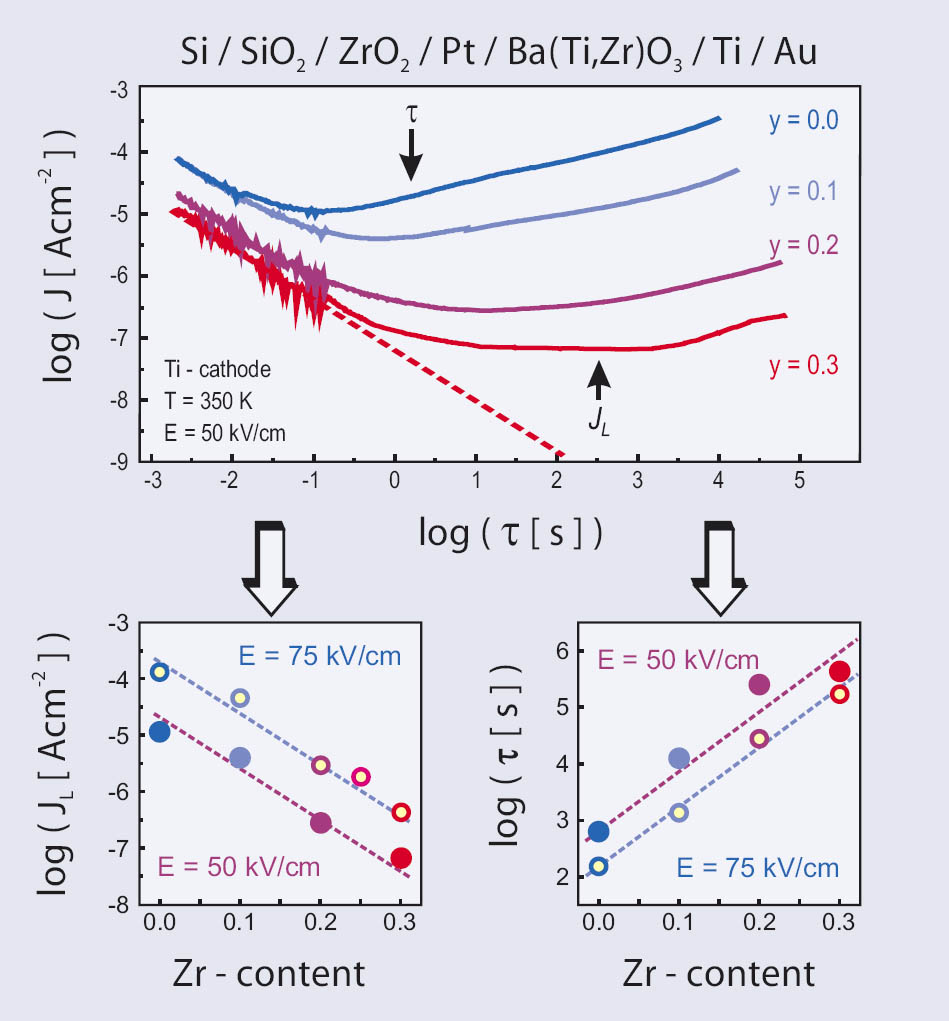
Figure 3: Leakage and resistance degradation behavior of 325 nm thick Ba(Ti1-yZry)O3 films with Ti/Au cathode for E = 50 kV/cm and T = 350 K
S. Hoffmann
Tunable and Switchable Mirowave Devices
Introduction
Electronically tunable and switchable microwave devices are always in demand if flexibility is desired. Tunable devices provide for new functionalities and enable the design of communication systems with reduced size and complexity. For example, a single tunable filter may replace a complete filter bank consisting of multiple different filters. Tunable antennas arranged as an array (phased array systems) can work together as a beam antenna with electronically adjustable beam alignment and beam angle. This can be achieved by using tunable phase-shifters for separate phase-control of each antenna feeding signal. Other important device examples are tunable impedance matching networks, which are needed to compensate frequent and rapid changes of the radiation resistance of portable systems (e.g. cell phones).
Various possibilities of providing tunability have been proposed in the literature. For example, tunable devices may employ semiconductor based varactors and switches, optical elements, liquid crystals, magnetic materials, ferroelectric materials, or micro-electromechanical systems (MEMS). All of these approaches differ in regard to the achievable tunability, loss contribution, linearity, tuning speed (switching rate), bias voltage, power consumption, microwave power-handling capability, cross sensitivities (dependence of temperature, vibrations, etc…), reliability, life cycle, area consumption, fabrication compatibilities (especially CMOS-compatibility), and fabrication cost. Thereby, the choice of the appropriate tuning method may depend on the specific application, where tunability is needed. Nevertheless, it is possible to assess the merit of a tuning element.
Figure of Merit of a Tuning Element
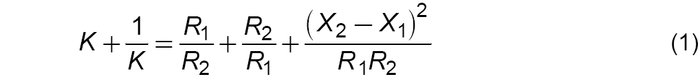
The achievable tunability and loss contribution of a tuning element are crucial parameters for its applicability in microwave devices. For a given tuning element, these two parameters cannot be altered independently from each other. This relation is taken into account by the Vendik's commutation quality factor (CQF) [1], which is used as figure-of-merit definition. Any tuning element or switch can be represented by a tunable or switchable impedance in equivalent circuits. Considering two achievable tuning states or switching sates of impedance with real and imaginary parts, i.e. Z1 = R1 + jX1, and Z2 = R2 + jX2, the commutation quality factor K is defined by equation (1):
Some conditions allow for simplifying the equation (1). If X1 ≈ X2 and K > 1000, then the CQF is approximately given by equation (2). This case applies to a switch, where R1 and R2 represent the contact resistance and isolation resistance, respectively.
If R1 ≈ R2 and K > 200, then the CQF is approximately given by equation (3). This case applies to a varactor or tunable inductor.
If a tuning element is employed within a circuit, the two above considered values of impedance (Z1 and Z2) may be transformed into different values. Thereby, the tunability or loss contribution may vary. However, it can be shown that the CQF is invariant to lossless reciprocal transformation. This means that the CQF remains constant for a given tuning element, even if the tuning element and additional lossless elements are interconnected in some way to form a different two-port network with different tuning or switching states of impedance. Therefore, the CQF is seen as the dominating criterion defining the figure of merit of a tunable element.
Based on the CQF, additional figure-of-merit definitions can be given for concrete devices like phase shifters and filters.
Ferroelectric Varactors as Tuning Elements
The permittivity of ferroelectric materials is dependent on the electric field intensity and can be biased by an applied DC-voltage. This property is utilized for designing voltage controlled variable capacitors, namely, ferroelectric varactors for tunable microwave applications. Even if classical ferroelectric materials are used, these materials are usually employed in the paraelectric phase in order to avoid any hysteresis effects. BaxSr(1-x)TiO3 (BST) is considered as the strongest candidate for developing tunable components based on ferroelectrics.
Ferroelectric materials are attractive due to sub-microsecond tuning speed and low fabrication costs. At microwave frequencies the performance (defined by the CQF) can be better than the one of semiconductor-based tuning elements. In contrast to MEMS-based components, ferroelectric varactors do not succumb to mechanically related problems, such as sensitivity to vibrations. The triplanar thin film varactors (parallel plate capacitors) fabricated at the EMRL benefit from DC-bias voltages as low as 10 V and exhibit a higher tunability than interdigital varactors. In contrast, thick film components or bulk ceramics require significantly higher bias-voltages which are generally not desired.
According to equation (5), the tunability (n) of a varactor is defined by the ratio of the achievable maximum (C1) and minimum (C2) of the variable capacitance.
Based on equation (3) the commutation quality factor can be given by equation (6) [1], where tan(δ1) and tan(δ2) are the loss tangents at the two tuning states of maximal and minimal capacitance, respectively.
Different loss contributions are responsible for the varactor loss at microwave frequencies. A detailed review of the dielectric response and the material related loss mechanisms is given in [2]. Current research on ferroelectric thin films is aimed at minimizing the extrinsic loss due to defects and coming up with loss tangents close to those of bulk materials. Another loss contribution is caused by sound emissions in the GHz range due to electrostrictive resonances [3], [4]. Therefore, also the acoustic properties have to be taken into account at designing thin film varactors. Furthermore, the electrode loss can make a significant contribution. For thin film varactors the electrode loss may exceed all other loss contributions.
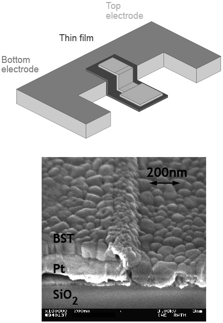
Figure 1:
Fig 1a) depicts the schematic design of a triplanar thin film varactor which consists of a BST-film sandwiched by two electrodes. Fig. 1b) shows a 100 nm thick Pt bottom electrode on top of a silicon substrate covered with a 100 nm thick BST-film deposited by CSD (chemical solution deposition). Due to the high permittivity of BST, the varactors have an area of only few μm2 at a typical capacitance of around 100 fF, such as required for applications working at frequencies higher than 10 GHz. Thereby, the thickness of the electrodes depends on the realizable aspect ratios. For the varactor design given in Fig. 1 a) and b), the thickness of the bottom electrode should not exceed the thickness of the BST-film. Otherwise, the edge of the bottom electrode is not covered anymore by the film. As thick electrodes are desired to keep the varactor loss low, different varactor designs and the required fabrication processes have to be developed.
Additional research is necessary to satisfy demands for temperature stability and linearity. Some possible solutions to compensate the temperature dependence are summarized in [5]. On account of linearity, the voltage swing of the microwave signal applied to a varactor should be kept as low as possible. This can be achieved by connecting a number of varactors in series. In order to preserve the tunability, each varactor can be connected to the DC-bias voltage through additional biasing resistors [6], [7]. Whereas a small biasing resistance degrades the quality factor of a varactor, a too large biasing resistance increases the time constant (τ = RC) and, hence, reduces the tuning speed. Thus, a compromise has to be found.
Device Example: Tunable Filters
Passive microwave filters contain a number of resonators, which are coupled in appropriate way. In the MHz range and at low GHz frequencies the resonators may consist of lumped elements, i.e. capacitors and inductors. At higher frequencies, the use of lumped elements is not appropriate due to the strong decrease of their quality factors with increasing frequency. Instead, resonators with spatially distributed capacitance and inductance are used. Thereby, the underlying theory for designing filters made of lumped elements can be transferred to distributed filters, no matter what type of resonator is employed. In the following, some typical design problems, limitations and challenges are addressed by considering tunable bandpass filters.
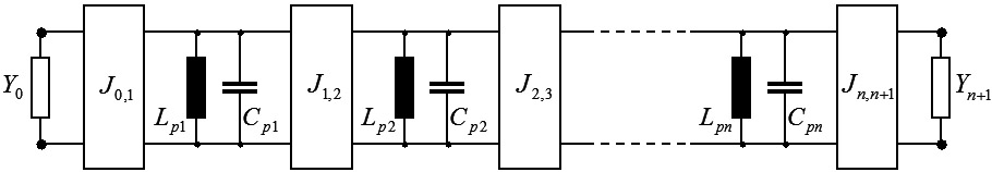
Figure 2:
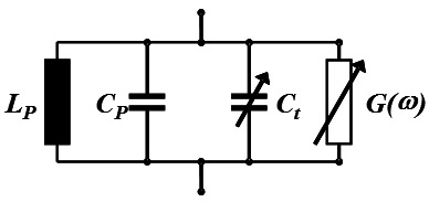
Figure 3:
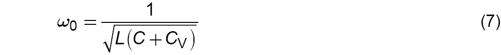
Fig 2 shows the equivalent circuit of an n-th order bandpass filter based on the common ladder-type filter structure. In the displayed equivalent circuit, different LC resonant circuits are coupled via J-Inverters, each of which represents a coupling network providing for appropriate coupling strength between the resonant circuits. The values Y0 and Yn+1 represent the input- and output-feed admittances. In order to make the center frequency tunable, varactors can be added to the LC resonant circuits as indicated in Fig. 3. The additional variable resistor in Fig. 3 represents the varactor loss, which can depend on the tuning state. According to the resonant frequency given by equation (7) the tunability of the center frequency can be calculated by using equation (8), where L is the inductance, C is the fixed capacitance, and CV is the varactor capacitance. Hence, the tunability of center frequency depends on the ratio of fixed and variable capacitance. The possible maximum of the tunability is given by equation (9). Due to requirements for design and implementation the tunability of center frequency is always lower than the maximum. With regard to the specific design of microwave resonators used in a microwave filter it may not be easy to achieve a high tunability.
Fig. 4a) shows the calculated insertion loss obtained for a 3rd order tunable bandpass filter under the assumption that all elements are lossless and that the varactors have a tunability of factor 2, whereas the center frequency is tunable by 25%. Moreover, it is assumed that the values of the parameters J0,1 to Jn,n+1 are proportional to frequency. The latter assumption corresponds to capacitive inter-resonator coupling. As seen in Fig. 4a) the bandwidth and the characteristics drastically depend on the tuning state. Fig. 4b) displays the tunable filter characteristics obtained for the same assumptions but for a varactor loss tangent of 0.05. As seen, the insertion loss significantly increases with decreasing bandwidth and the passband is not shaped uniformly at different tuning states. This example illustrates that additional efforts are necessary to realize tunable filters with good performance. The reduction of bandwidth with down-tuned center frequency is due to the frequency dependencies of the external quality factors and of the J-inverters. Various possibilities of realizing the inverters with different behavior are known. Thereby, a different dependence of bandwidth can be achieved. One possibility of designing filters with preserved bandwidth is given by using tunable J-inverters though it may yield additional loss. Using more sophisticated resonators and coupling networks with appropriate frequency dependencies allows for approximately preserving the bandwidth at tuning the center frequency.
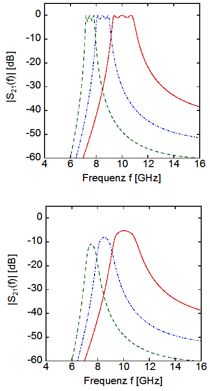
Figure 4:
The equations (3), (4) and (6) indicate a trade-off between varactor loss and varactor tunablity. Similarly, there is a trade-off between insertion loss and tunability of bandpass filters, too. Pleskachev and Vendik [8] have proposed a figure of merit definition for tunable filters, which is given in equation (10). In equation (10) F denotes the figure of merit of a tunable bandpass filter, ω0,max and ω0,min denote the maximal and minimal possible center frequencies, whereas Δω(ω0,max) and Δω(ω0,min) are the bandwidths at maximal and minimal center frequency, L(ω0,max) and L(ω0,min) is the insertion loss in dB at maximal and minimal center frequency, respectively, and N is the filter order. It shows that the demand for low insertion loss is contradictory to the demand for high relative tunability.
For standard Chebychev filters it can be shown [8] that the figure of merit only depends on the CQF of the employed varactors, as given by equation (11), where K is the CQF and N is the filter order.
One important parameter, which is not taken into account by the equations (10) and (11), is the area consumption. Miniaturization is of strong industrial concern, and it is known that miniaturization generally leads to an increase of loss. It is frequently reported that ferroelectric materials provide for considerable possibilities of miniaturization due to their high permittivity. Indeed, it could be concluded that the price of loss is not only paid for tunability but also for miniaturization, if appropriate designs can be developed. This could push tunable ferroelectrics into a new light. Moreover, a number of multiple tunable filters could be combined to achieve a higher additive tunability. On the one hand, this possibility could show a way to evade the limitations given by equation (11) but on the other hand, the multiple of area would be needed. This, in turn, suggests that the area consumption is a crucial parameter, which should to be taken into account when considering design limitations.
Several implementations of tunable filters with preserved bandwidth and constant characteristics are described in the literature, e.g. [9]. However, often systematic design procedures are missing, and, mostly, the described implementations are only available in a certain technology, e.g. as microstrip circuit or as coplanar waveguide (CPW) structure. Additional constraints are given by limits of bandwidth, working frequency and realized tunability. Important issues such as the need for linearity, small filter size, or possibilities of miniaturization are generally not considered. Thus, the available implementations of tunable filters succumb to a lack of general applicability, and the design of varactor tuned filters with good performance remains challenging.
The EMRL focuses on developing tunable CPW-filters with regard to the listed design problems and possibilities.
Piezoelectrically actuated MEMS-Switches and Applications
An additional approach under investigation is the development of piezoelectrically actuated MEMS-switches used for reconfigurable microwave applications. In comparison to electrostatic MEMS-switches, piezoelectric MEMS-switches require significantly lower bias voltages (below 10 V) und do not suffer from stiction of electrodes, which can limit the life time. Fig 5 shows the design principle of a piezoelectric micro-relay bridge structure. Depending on the value of the bias voltage applied to the displayed SiO2/Pt/PZT/PT stack, the bridge is bent up or down in order to interconnect or release the two displayed contact bars. It is believed that such a design can handle relatively large signal powers and exhibits relatively high mechanical stability compared to other switch designs.
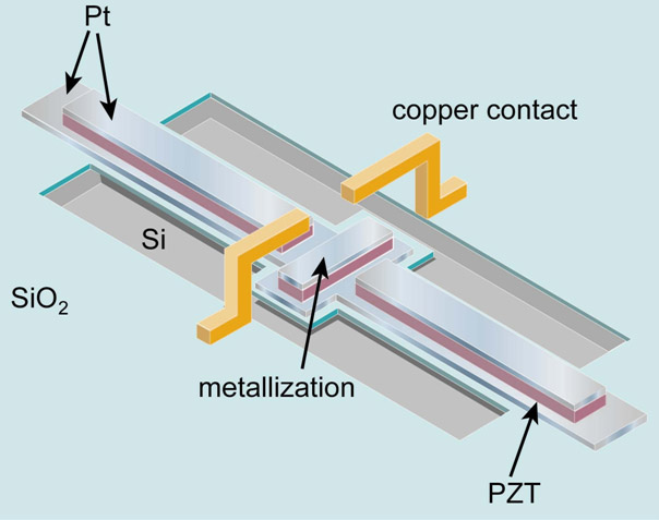
Figure 5:
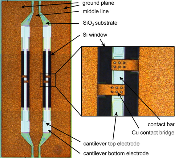
Figure 6:
Fig. 6 shows two fabricated micro-relays, which are similarly shaped as shown in Fig. 5 and integrated into a coplanar waveguide (CPW) transmission line. A CPW transmission line is formed of a middle conductor separated from a pair of groundplanes on top of a dielectric substrate. Due to the in-plane surface metallization of the CPW, no vias are required to interconnect the groundplanes with other conducting areas. Therefore, CPW structures provide for convenient possibilities of integration with the aid of surface micromachining. CPW structures have attracted an increased attention in the last decade. Microwave devices based on CPW structures are reported to offer some advantages compared to devices based on other structures, e.g. microstrip structures. Attractive features are the reduced sensitivity to the substrate thickness, low dispersion, the wide range of realizable characteristic impedance, and wide frequency range of use [10].
If the bridges of the micro-relays in Fig 6 are bent up, the design shown in Fig 6 corresponds to a closed shunt switch, which blocks the wave propagation along the CPW line. If the bridges are bent down, the microwave signal can pass without significant attenuation. In order do design a shunt switch with good performance the contact resistance should be kept as low as possible, since the desired isolation obtained for closed switches is significantly degraded with increasing contact resistance. Apart from this, the isolation is degraded with increasing frequency, too. One possibility to avoid this degradation is given using resonant structures combined with MEMS switches. Disadvantages of this approach are the increased area consumption due to the resonator size and the narrow bandwidth associated with the use of resonators. Alternatively, it is possible to cascade a number of switches separated in certain distances from each other in order to enhance the isolation. Likewise, this approach consumes additional area, too.
Apart from the investigation of different material systems and fabrication processes, different applications, such as switches, phase shifters and filters based on coplanar waveguide (CPW) structures are developed at the EMRL. Considering MEMS-reconfigurable filters, the typical design problems and challenges are similar to those described above for varactor tuned filters.
- [1] I.B. Vendik, O.G. Vendik, E.L. Kollberg, “Commutaion Quality Factor of two-State Switchable Devices”, IEEE Trans. MTT., Vol. 48 No. 5, pp. 802-808, May 2000.
- [2] A.K. Tagantsev, V.O. Sherman, K.F. Astafiev, J. Venkatesh, N. Setter, “Ferroelectric Materials for Tunable Microwave Applications”, Journal of Electroceramics, 11, pp. 5-66, 2003.
- [3] S. Tappe, U. Böttger, R. Waser, “Electrostrictive resonances in (Ba0.7Sr0.3)TiO3 thin films at microwave frequencies”, Appl. Phys. Letters, Vol. 58 No. 4, July 2004.
- [4] S. Gevorgian, A. Vorobiev, T. Lewin, “DC filed and temperature dependent acoustic resonances in parallel plate capacitors based on SrTiO3 and Ba0.25Sr0.75TiO3 films: Experiment and modeling”, J. of Appl. Phys. 99, 2006.
- [5] N. Setter, D. Damjanovic, et al., “Ferroelectric thin films: Review of Materials and Applications”, J. of Appl. Phys. 100, 2006.
- [6] P. Scheele, A. Giere, Y. Zheng, F. Goelden, R. Jakoby, “Modeling and Applications of Ferroelectric-Thick Film Devices with Resistive Electrodes for Linearity Improvement and Tuning Voltage Reduction”, IEEE Trans. MTT., Vol. 55 No. 2, pp. 383-390, Feb 2007.
- [7] J.-S. Fu, X.A. Zhu, J.D. Phillips, A. Mortazawi “Improving Linearity of Ferroelectric-Based Microwave Tunable Circuits”, IEEE Trans. MTT., Vol. 55 No. 2, pp. 354-360, Feb 2007.
- [8] V. Pleskachev, I. Vendik, “Figure of Merit of Tunable Ferroelectric Planar Filters”, 33rd EuMC Conference Proceedings, 2003.
- [9] G. Torregrosa-Penalva, G. Lopez Risueno, J.L. Alonso, “A Simple Method to Design Wideband Electronically Tunable Combline Filters”, IEEE Trans. MTT., Vol. 50 No. 1, pp. 172-177, Jan 2002.
- [10] Ingo Wolff, “Coplanar Microwave Integrated Circuits”, Wiley, Hoboken, New Jersey, USA.
Alexander Hennings, Carsten Dehoff, Carsten Kügeler