Integration of TiO2 into Nano-Crossbar Arrays with 100 nm Half Pitch for Resisitve RAM Applications
Non-volatile resistively switching TiO2 is integrated into nano-crossbar arrays and nano-cross-points scaled down to a feature size of 100 nm by electron beam lithography. This represents fast fabrication route for high density prototype test structures of passive memory cores with two terminal devices. The structures and the integrated material is electrically characterized to gain an insight into the general properties of nano-crossbar arrays with resistively switching TiO2 and to define the demands for an external CMOS control system.
The persistent increase of memory integration density expressed by Moore’s law illustrates the demand for ever smaller structures: Nano-crossbar arrays are therefore widely investigated [1]. Nonvolatile and resistively switching materials with two stable states such as TiO2 are integrated as two terminal memory devices to efficiently create a RRAM bit pattern [2,3]. Figure 1 illustrates how these cells are integrated into crossbar arrays where the simple design reduces the cell size per bit to 4 F2. The switching material covers the whole chip area and every junction at a cross point is an addressable cell of a RRAM. Since the array consists of passive elements, additional active external circuitry is required for the operation to address the cells, set and reset their state and read the stored information [4,5].
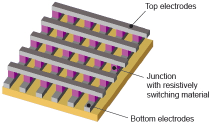
Figure 1: Pattern of a crossbar array. The metallic top and bottom electrode (grey) sandwich the functional layer (pink) of a resistively switching material which is only illustrated at the junctions.
We report on a novel fabrication route to create crossbar arrays in the nanometer range. Structures of Pt electrodes with resistively switching TiO2/Ti layers offer a model system to study the properties of passive crossbar arrays and the specific requirement of these systems concerning external control structures for a CMOS hybrid.
ALD deposited TiO2 showed promising, non-volatile switching characteristics in micro structures and is convenient to integrate at low temperature [6]. Additionally, the material is temperature stable and compatible with CMOS devices. As a proof of concept a 50 nm thick TiO2 layer was deposited via rf-sputtering of Ti in an oxygenated atmosphere [7]. The layer was integrated into photo lithographically structured micro-crosspoints with 50 nm thick Pt electrodes fabricated via a lift-off process. Figure 2 shows the current response of a pulse pattern for a 1 × 1 µm² crosspoint structure. Extended investigations confirm the promising resistive switching properties of the material for 6000 cycles, illustrated in Figure 3.
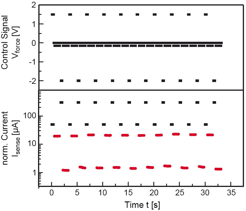
Figure 2: Pulse pattern measurement. The set/reset voltages were 1.5 V and −2 V (upper graph), respectively, and both signals were limited at 50 µA and −300 µA. Pulse duration was 300 ms. The read voltage amounted to −0.15 V without any current limit, and the corresponding response was around 20 µA for ‘1’ state and 2 µA for ‘0’ state, respectively (lower graph). Here, pulse duration was 150 ms.
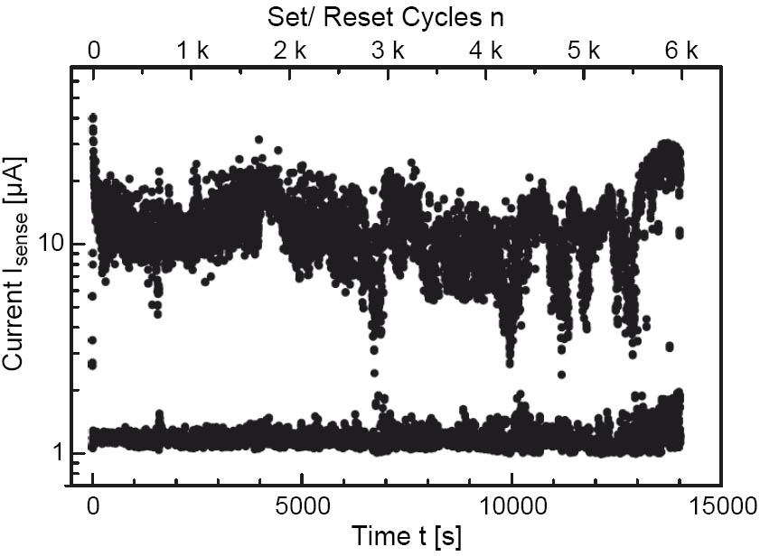
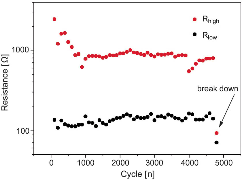
Figure 3: Endurance test with 300 ms pulses. The cell was tested for 6000 cycles with 1 set, 3 read, 1 reset and 3 read pulses.
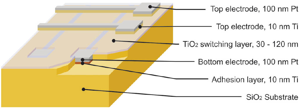
Electron Beam Lithography in combination with a lift-off process is used to fabricate prototype test crossbar structures with a feature size of 100 nm (Figure 3). The lift-off process forms the metal electrodes using a two layer resist on a 1” × 1” SiO2 substrate. The bottom resist is a copolymer PMMA/MA with a thickness of 60 nm and the top resist is a PMMA polymer with a thickness of 25 nm. An electron beam dose of 200 μC cm−2 is necessary to write the 100 nm lines in the resist in order to expose the substrate along the specified structure during the development. As the copolymer is more sensitive to the electron beam than the polymer, this results in a larger expansion of the resist gap of the bottom layer, respectively a staged overhanging resist edge. This is mandatory for well defined metal structures after lift-off and in consequence no additional etching process is required to remove the residual resist in the gap. A combination of 5 nm Ti as adhesion layer with a 20 nm Pt film, which is deposited by electron beam evaporation serves as electrode material. Subsequently a non structured 30 nm thick TiO2 layer is sputtered as abovementioned. Finally, the electron beam lithography and the lift-off process are repeated to create the orthogonally arranged top electrode structures. The fabricated structures comprise single cells (1 × 1 bit), words (1 × n bit) and arrays (n × n bit) with half pitches down to 100 nm and sizes of n = 8, 16, 32 and 64 (Figure 4).
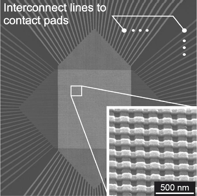
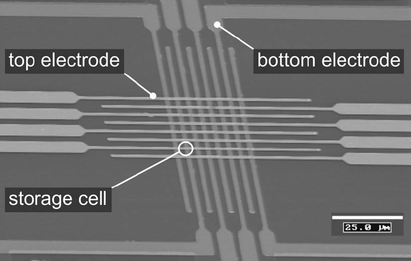
Figure 4: SEM picture of 64 × 64 bit nano-crossbar array with 100 nm half-pitch. The SEM inspection showes no structural defect within the array.
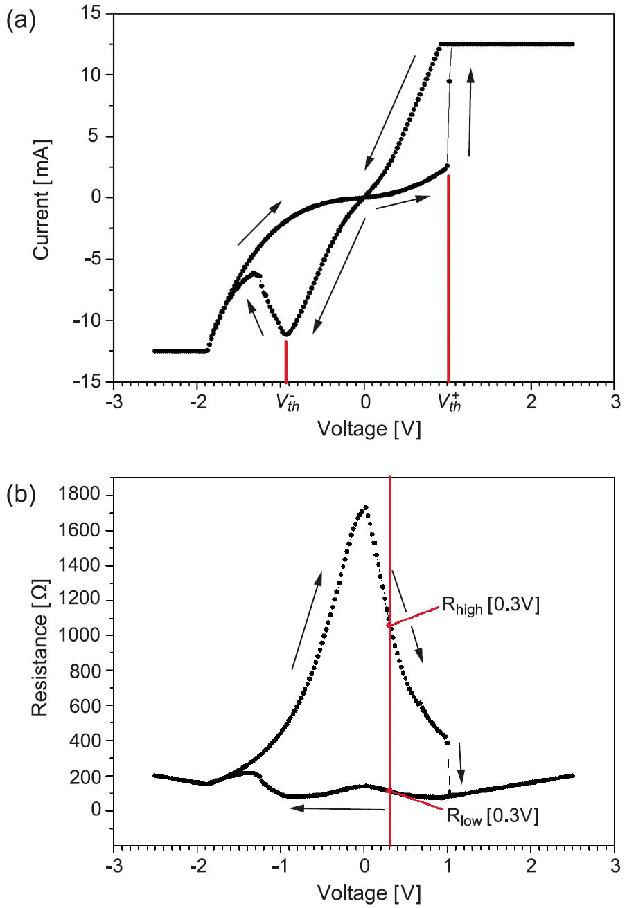
To get a general understanding of the resistively switching in the integrated TiO2 layer we characterized a single 100 × 100 nm² cell. The initial state of the cell is high resistive with a resistance of several GΩ and a diode like behavior. A current driven electroforming process with an increasing current (10 nA s−1) initializes the cell into the low resistive ‘ON’ state. Under this condition the cell exhibits a non-linear I(V) characteristic shown in Figure 5a. The corresponding R(V) curve is shown in Figure 5b. A negative voltage switches the cell to the high resistive, respectively ‘OFF’-state by exceeding a certain threshold value Vth−. This ‘OFF’ state differs for several orders of magnitude from the initial state and is also non-linear. To switch back into the ‘ON’-state, the polarization is changed and a positive threshold Vth+ has to be exceeded. A current limiter prevents the cell from a destructive electrical breakdown at 30 μA which leads to an abrupt jump in the I(V) curve. A nondestructive readout of the cell is performed by voltages within the range from Vth− to Vth+, and the resistance condition is nonvolatile even if no supply voltage is applied. In Figure 5b a read out voltage of 0.3 V exemplifies a resistance of 1.275 MΩ for the ‘OFF’-state and 36.274 kΩ for the ‘ON’-state corresponding to a ratio of 35. The high resistance ratio in combination with a high RON value and the feature of current determined readout instead of charge determination accommodates the demands for a CMOS hybrid.
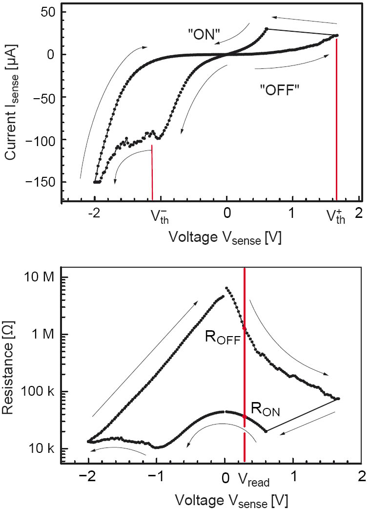
Figure 5: I(V) characteristic of a single 100 × 100 nm² cell measured via Kelvin probing. (b) R(V) curve corresponding to Figure 5 a.
We fabricated nano-crossbar arrays by electron beam direct writing and integrated resistively switching TiO2. By downscaling to feature sizes of 100 nm we create addressable patterns with sizes up to 4096 bit and a potential density of 2.5 Gbit cm−2. Single memory cells were electrically characterized and showed non-volatile bipolar resistance switching. The electrical characterization was done in sweep as well as in pulse mode with. The electrical properties fulfill the demands for an integration and characterization of resistively switching materials.
- [1] J. E. Green, J. W. Choi, A. Boukai, Y. Bunimovich, E. Johnston-Halperin, E. DeIonno, Y. Luo, B. A. Sheriff, K. Xu, Y. S. Shin, H.-R. Tseng, J. F. Stoddart, J. R. Heath, Nature 445, 414–417 (2007)
- [2] A. Beck, J. G. Bednorz, Ch. Gerber, C. Rossel, D. Widmer, Appl. Phys. Lett. 7, 139–141 (2001)
- [3] R. Waser, M. Aono, Nature Materials 6, 833–840 (2007)
- [4] J. Mustafa, and R. Waser, IEEE Trans. Nanotechn. 5, 687–691 (2006)
- [5] A. Flocke, T. G. Noll, in 33rd European Solid-State Circuits Conference, Munich 2007, 328–331
- [6] C. Nauenheim, T. Watanabe, C. Kügeler, A. Rüdiger, R. Waser, 2nd Workshop on Integrated Electroceramic Functional Structures, Berchtesgaden, (2007)
- [7] D. S. Jeong, H. Schroeder, R. Waser, Appl. Phys. Lett. 89, 2909–13 (2006)
C. Nauenheim, R. Rosezin, C. Kügeler, A. Rüdiger, S. Trellenkamp, R. Waser